Hardware Reference Manual 363
Intel
®
IXP2800 Network Processor
Clocks and Reset
10.2 Synchronization Between Frequency Domains
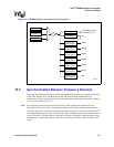
Due to the internal design architecture of the IXP2800 Network Processor, it is guaranteed that one
of the clock domains of an asynchronous transfer will be the Push/Pull domain (PLL/4).
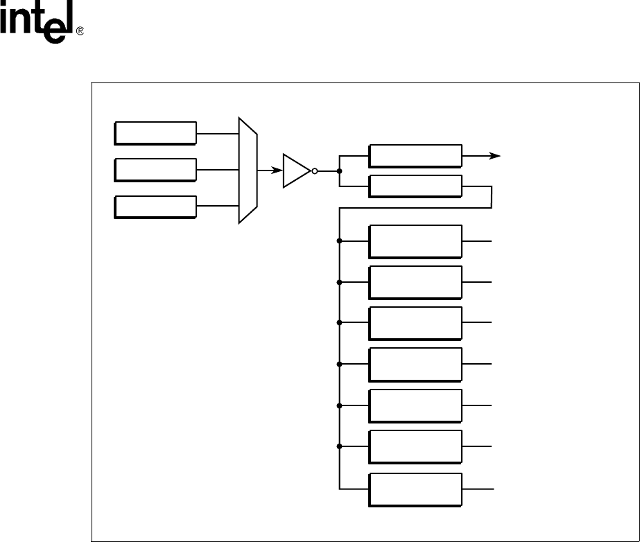
Additionally, all other clocks are derived by further dividing the Microengine clock (PLL/2n where
n is 3 or more); refer to Figure 132.
Note: The exception is the PCI unit where the PCI clock is fully asynchronous with the PP clock.
Therefore in the PCI unit, data is synchronized using the usual 3-flop synchronization method.
Therefore, the clock A and clock B relationship will always be apart by at least two PLL clocks. To
solve hold problem between clock A and clock B, a delay is added anytime data is transferred from
clock A to clock B. The characteristic of this delay element is such that it is high enough to resolve
any hold issue in fast environment but in the slow environment its delay is still less than two PLL
clocks.
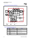
Figure 131. IXP2800 Network Processor Clock Generation
A9778-04
PLL
Bypass Clk
DFT TBD
Divide by 4
ME
DRAMs
SRAM0
SRAM1
SRAM2
SRAM3
MEDIA
APB
Internal Buses (CPP),
Intel XScale
®
Core
Divide by 2
Divide by N
(reset value: 15)
Divide by N
(reset value: 15)
Divide by N
(reset value: 15)
Divide by N
(reset value: 15)
Divide by N
(reset value: 15)
Divide by N
(reset value: 15)
Divide by Nx4
(reset value: 15)


