182 Hardware Reference Manual
Intel
®
IXP2800 Network Processor
Microengines
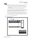
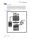
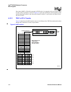
4.5.1.2 Write to TBUF
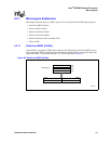
Data in TBUF is arranged in LWBE order. When writing from the Microengine transfer registers to
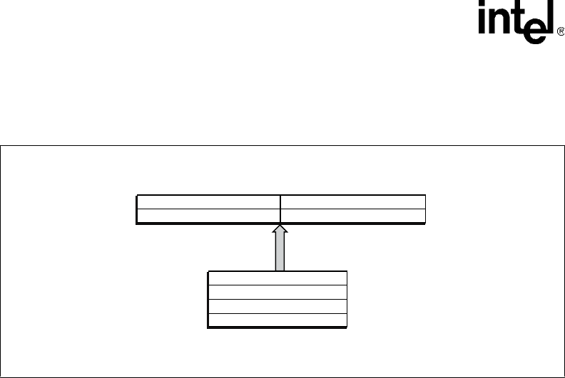
TBUF, treg0 goes into LDW0, treg1 goes into LDW1, etc. See Figure 61.
4.5.1.3 Read/Write from/to SRAM
Data inside SRAM is in big-endian order. While transferring data from SRAM to a Microengine,
no endianness is involved and first read data goes into the first transfer register specified, the next
read data into the second, etc.
4.5.1.4 Read/Write from/to DRAM
Data inside DRAM is in LWBE order. When a Microengine reads from DRAM, LDW0 goes into
the first transfer register specified in the instruction, LDW1 goes into the next, and so on. While
writing to DRAM, treg0 goes first, then followed by treg1, and both are combined in the DRAM
controller as {LDW1, LDW0} and written as a 64-bit quantity into DRAM.
4.5.1.5 Read/Write from/to SHaC and Other CSRs
Read and write from SHaC and other CSRs happen as 32-bit operations only and are endian-
independent. The low byte goes into the low byte of the transfer register and the high byte goes into
the high byte of the transfer register.
Figure 61. Write to TBUF (64 Bits)
A8942-01
0123
4567
8 9 10 11
12 13 14 15
4567
12 13 14 15
MicroEngine
treg0
treg1
treg2
treg3
0123
8 9 10 11
TBUF


