142 Hardware Reference Manual
Intel
®
IXP2800 Network Processor
Intel XScale
®
Core
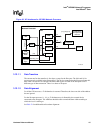
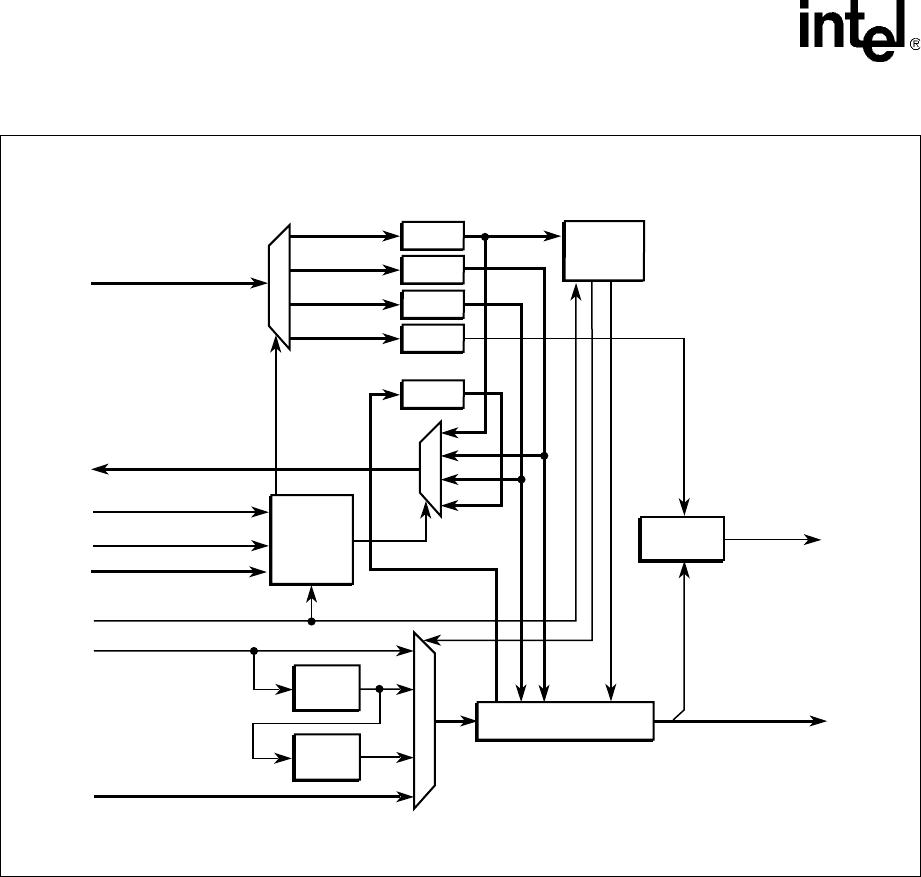
Figure 34 shows the Timer Internal logic.
3.12.7 Slowport Unit
The IXP2800 Network Processor Slowport Unit supports basic PROM access and 8-, 16-, and
32-bit microprocessor device access. It allows a master, (Intel XScale
®
core or Microengine), to do
a read/ write data transfer to these slave devices.
The address bus and data bus are multiplexed to reduce the pin count. In addition, the address bus
is also compressed from A[25:0] down to A[7:0] and shifted out with three clock cycles. Therefore,
an external set of buffers is needed for address storage and latch.
The access can be asynchronous. Insertion of delay cycles is possible for both setup and hold data.
A programmable timing control mechanism is provided for this purpose. There are two types of
interfaces supported in the Slowport Unit:
• Flash memory interface
• Microprocessor interface.
Figure 34. Timer Internal Logic Diagram
A9703-01
WRITE_DATA
ADDRESS
APB_WR
ENABLE
CLK
GP_TM[3:0]
READ_DATA
Watchdog
Reset
Interrupts
TCTL
Divided
by 16
Divided
by 16
Timer
Control
Logic
Decoder
& Control
Logic
Watchdog
Logic
Counter Logic
Timer Registers
Block
TCLD
TCLR
APB_SEL
TWDE
TCSR


