Hardware Reference Manual 153
Intel
®
IXP2800 Network Processor
Intel XScale
®
Core
16-Bit Microprocessor Write Interface Protocol
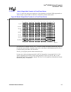
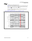
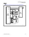
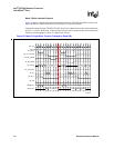
Figure 43 uses the Lucent* TDAT042G5 device. In this case, the user should program the P_PCR
register to mode 1 and also program the write timing control register to setup=7, pulse width=5,
and hold=1, which represent seven clock cycles for CS
, five clock cycles for DT delay, and one
clock cycle for ADS
. They are intervened with two idle cycles.
From Figure 43, we observe that there are a total of twelve clock cycles used for write access,
(i.e., 240 ns), not including an intervened turnaround cycle after the write transaction. The
throughput is 8.3 Mbytes per second.
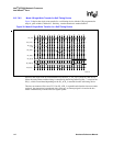
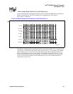
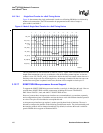
Figure 43. Mode 1 Single Write Transfer for Lucent* TDAT042G5 Device (B0)
B1742-04
SP_CLK
SP_ALE_L
SP_CS_L[1] /CS#
SP_WR_L/ADS#
SP_RD_L/R/W#
2
T0 T1 T2 T3 T4 T0 T1 T2 T3 T4T5 T6
0 4 6 8 10 12 14 16 18 20
SP_AD[7:0]
SP_ACK_L /DT#
SP_CP
SP_OE_L
D[15:0]
A[23:0] A[23:0]
SP_DIR
ADDR[15:0]
DATA[15:0]
A
[15:0]
A
[15:8]
A
[7:0]
A
[23:16]
A
[15:8]
A
[7:0]
A
[23:16]
D
[7:0]
D[15:8]
D
[7:0]
A
[15:0]
A
[7:0]
A
[7:0]


