Hardware Reference Manual 83
Intel
®
IXP2800 Network Processor
Intel XScale
®
Core
3.3.1.2.2 Instruction Cache
When examining these bits in a descriptor, the Instruction Cache only utilizes the C bit. If the C bit
is clear, the Instruction Cache considers a code fetch from that memory to be non-cacheable, and
will not fill a cache entry. If the C bit is set, then fetches from the associated memory region will be
cached.
3.3.1.2.3 Data Cache and Write Buffer
All of these descriptor bits affect the behavior of the Data Cache and the Write Buffer.
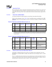
If the X bit for a descriptor is 0 (see Table 20), the C and B bits operate as mandated by the ARM*
architecture. If the X bit for a descriptor is one, the C and B bits’ meaning is extended, as detailed
in Table 21.
3.3.1.2.4 Details on Data Cache and Write Buffer Behavior
If the MMU is disabled all data accesses will be non-cacheable and non-bufferable. This is the
same behavior as when the MMU is enabled, and a data access uses a descriptor with X, C, and B
all set to 0.
The X, C, and B bits determine when the processor should place new data into the Data Cache. The
cache places data into the cache in lines (also called blocks). Thus, the basis for making a decision
about placing new data into the cache is a called a “Line Allocation Policy.”
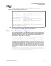
Table 20. Data Cache and Buffer Behavior when X = 0
C B Cacheable? Bufferable? Write Policy
Line
Allocation
Policy
Notes
0 0 N N — — Stall until complete
1
1. Normally, the processor will continue executing after a data access if no dependency on that access is encountered. With
this setting, the processor will stall execution until the data access completes. This guarantees to software that the data ac-
cess has taken effect by the time execution of the data access instruction completes. External data aborts from such access-
es will be imprecise.
0 1 N Y — —
1 0 Y Y Write Through Read Allocate
1 1 Y Y Write Back Read Allocate
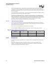
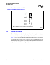
Table 21. Data Cache and Buffer Behavior when X = 1
C B Cacheable? Bufferable? Write Policy
Line
Allocation
Policy
Notes
0 0 — — — — Unpredictable; do not use
0 1 N Y — —
Writes will not coalesce into
buffers
1
1. Normally, bufferable writes can coalesce with previously buffered data in the same address range
1 0
(Mini Data
Cache)
———
Cache policy is determined
by MD field of Auxiliary
Control register
1 1 Y Y Write Back
Read/Write
Allocate


