Hardware Reference Manual 149
Intel
®
IXP2800 Network Processor
Intel XScale
®
Core
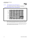
3.12.7.6.3 Mode 0 Single Read Transfer for Fixed-Timed Device
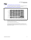
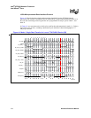
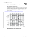
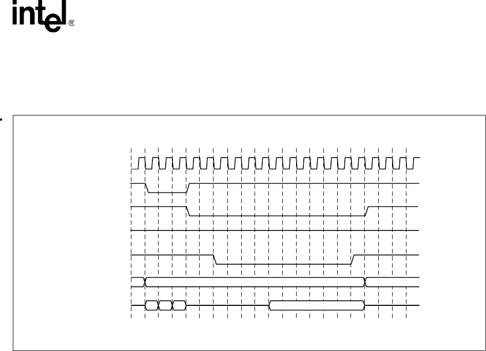
Figure 40 demonstrates the single read transfer issued to a fixed-timed PROM device followed by
another write transaction. The CSR is assumed to be configured to the value setup=2,
pulse width=10, and hold=1.
The address is loaded onto the external buffer in three clock cycles with the ALE_L asserted. Then,
a clock cycle is inserted to tri-state all the AD[7:0] signals. The CS_L[1:0] signals come asserted
on the fourth clock cycle. Now, the values stored in the timing control registers take effect. The
RD_L is asserted after two clock cycles. It keeps asserted for ten clock cycles. The CS_L[1:0]
should be de-asserted one clock cycle after RD_L is de-asserted. The data will be valid at clock
cycle 16 as shown in the diagram. Since the hold delay has two cycles, and the transaction is
terminated at clock cycle 16.
Figure 40. Mode 0 Single Read Transfer for Fixed-Timed Device
A9708-02
SP_CLK
SP_ALE_L
SP_CS_L
[1:0]
SP_WR_L
D[7:0]
A[1:0]
A
24:18
A
17:10
A9:2
SP_RD_L
SP_A[1:0]
SP_AD[7:0]
20 4 6 8 10 12 14 16 18 20


