334 Hardware Reference Manual
Intel
®
IXP2800 Network Processor
PCI Unit
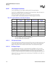
9.3.2.2 SRAM Slave Reads
For a slave read from SRAM, a 32-bit DWORD is fetched from the memory for memory read
command, one cache line is fetched for memory read line command, and two cache lines are read
for memory read multiple command. Cache line size is programmable in the CACHE_LINE field
of the PCI_CACHE_LAT_HDR_BIST configuration register. If the computed read size is greater
than 64 bytes, the PCI SRAM read will default to the maximum of 64 bytes. No pre-fetch is
supported in that the PCI Unit will not read beyond the computed read size.
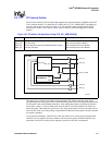
The PCI core resets the target read FIFO before issuing a memory read data request on FBus. The
maximum size of SRAM data read is 64 bytes. The PCI core will disconnect at the 64-byte address
boundary.
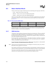
9.3.3 DRAM Interface
The memory is accessed using the push/pull mechanism. Request to memory is sent on the
command bus. If the PCI_DRAM_BAR is used, the target state machine generates a request to the
command bus for DRAM access with the address in the slave address FIFO. Once the push/pull
request is received. The data is directed between the Slave FIFOs of the PCI core and DRAM push/
pull bus.
9.3.3.1 DRAM Slave Writes
The slave write buffer is used to support memory burst accesses. The buffer is added to guarantee
data transfer for each clock and burst size can be determined before memory request is issued. Data
is assembled in the buffers before being sent to memory for memory write.
DRAM target write access is only required to be 8-byte address aligned and the address does not
wrap around the 64-byte address boundary on a DRAM burst. Each 8-byte access that is a partial
write to the memory, is treated as single write. Remaining writes of the 64-byte segment is written
as one single burst. Transfers that cross a 64 -byte segment are split into separate transfers.
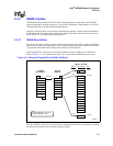
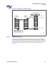
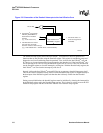
Figure 123 splits the 68-byte transfers into two partial 8-byte transfers to address 06 and address 48
and one 56-byte burst transfer in the first 64-byte segment from address 08 to 38 and one 8-byte
transfer to address 40.
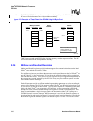
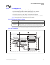
For write to DRAM on the push/pull bus, the burst must be broken down into address aligned
smaller transfer sizes (see Figure 122).
The Target interface also must make sure there is enough data in the target write buffer to complete
the memory data transfer before making a memory request.


