52 Hardware Reference Manual
Intel
®
IXP2800 Network Processor
Technical Description
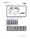
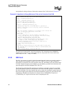
2.5.1 QDR Clocking Scheme
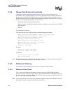
The controller drives out two pairs of K clock (K and K#). It also drives out two pairs of C clock
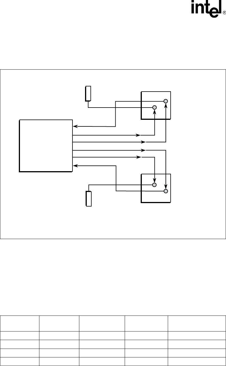
(C and C#). Both C/C# clocks externally return to the controller for reading data. Figure 8 shows
the clock diagram if the clocking scheme for QDR interface driving four SRAM chips.
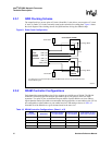
2.5.2 SRAM Controller Configurations
Each channel has enough address pins (24) to support up to 64 Mbytes of SRAM. The SRAM
controllers can directly generate multiple port enables (up to four pairs) to allow for depth
expansion. Two pairs of pins are dedicated for port enables. Smaller RAMs use fewer address
signals than the number provided to accommodate the largest RAMs, so some address pins (23:20)
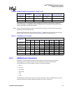
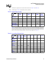
are configurable as either address or port enable based on CSR setting as shown in Table 10.
Note that all of the SRAMs on a given channel must be the same size.
Figure 8. Echo Clock Configuration
B3664-01
Clam-shelled SRAMS
CQ/CQ#
CQ/CQ#
Package Balls
Package Balls
Termination
Intel
®
IXP2800
Network
Processor
QDRn_CIN[0]
QDRn_K[0]
K/K#
K/K#
C/C#
C/C#
QDRn_C[0]
QDRn_K[1]
QDRn_C[1]
*QDRn_CIN[1]
Termination
*The CIN[1] pin is not used internally to capture the READ data; however, the I/O Pad can be used
to terminate the signal.
Table 10. SRAM Controller Configurations (Sheet 1 of 2)
SRAM
Configuration
SRAM Size
Addresses Needed
to Index SRAM
Addresses Used
as Port Enables
Total Number of Port
Select Pairs Available
512K x 18 1 MB 17:0 23:22, 21:20 4
1M x 18 2 MB 18:0 23:22, 21:20 4
2M x 18 4 MB 19:0 23:22, 21:20 4
4M x 18 8 MB 20:0 23:22 3


