Hardware Reference Manual 263
Intel
®
IXP2800 Network Processor
Media and Switch Fabric Interface
8.3.2 TBUF
The TBUF is a RAM that holds data and status to be transmitted. The data is written into sub-
blocks referred to as elements, by Microengine or the Intel XScale
®
core. TBUF contains a total of
8 Kbytes of data, and associated control.
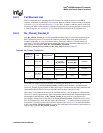
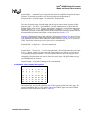
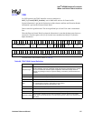
Table 95 shows the order in which data is written into TBUF. Each number represents a byte, in
order of transmission onto the tx interface. Note that this is reversed on a 32-bit basis relative to
RBUF — the swap of 4 low bytes and 4 high bytes is done in hardware to facilitate the
transmission of bytes.
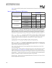
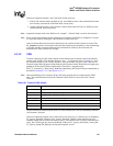
The mapping of elements to address offset in TBUF is based on the TBUF partition and element
size, as programmed in MSF_Tx_Control CSR. TBUF can be partitioned into one, two, or three
partitions based on MSF_Tx_Control[TBUF_Partition]. The mapping of partitions to transmit
data is shown in Table 96.
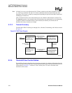
The data in each segment is further broken up into elements, based on
MSF_Tx_Control[TBUF_Element_Size_#] (n = 0,1,2). There are three choices of element size:
64, 128, or 256 bytes.
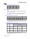
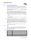
TPAR Output Not Used RTxPar
TSCLK Input TSCLK Not Used
TSTAT[1:0] Input TSTAT[1:0] Not Used
Table 94. Transmit Pins Usage by Protocol (Sheet 2 of 2)
Name Direction SPI-4 Use CSIX Use
Table 95. Order in which Data is Transmitted from TBUF
Data/Payload Address Offset (Hex)
01234567 0
89ABCDEF 8
10 11 12 13 14 15 16 17 10
Table 96. Mapping of TBUF Partitions to Transmit Protocol
Number of
Partitions
in Use
Transmit Data
Protocol
Data Use by Partition, Fraction of TBUF Used, Start Byte Offset (Hex)
Partition Number
012
1 SPI-4 only
SPI-4
All
Byte 0
n/a n/a
2 CSIX only
CSIX Data
3/4 of TBUF
Byte 0
CSIX Control
1/4 of TBUF
Byte 0x1800
n/a
3
Both SPI-4 and
CSIX
CSIX Data
1/2 of TBUF
Byte 0
SPI-4
3/8 of TBUF
Byte 0x1000
CSIX Control
1/8 of TBUF
Byte 0x1C00


