


User’s Manual
PPC440x5 CPU Core Preliminary
Page 128 of 589
cache.fm.
September 12, 2002
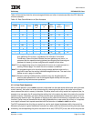
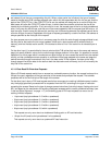
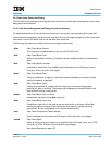
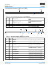
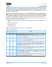
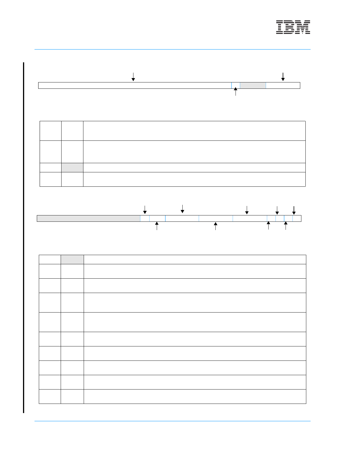
The following figures illustrate the DCDBTRH and DCDBTRL.
Figure 4-10. Data Cache Debug Tag Register High (DCDBTRH)
0:23 TRA Tag Real Address
Bits 0:23 of the lower 32 bits of the 36-bit real
address associated with the cache line read by
dcread.
24 V
Cache Line Valid
0 Cache line is not valid.
1 Cache line is valid.
The valid indicator for the cache line read by
dcread.
25:27 Reserved
28:31 TERA Tag Extended Real Address
Upper 4 bits of the 36-bit real address associated
with the cache line read by dcread.
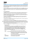
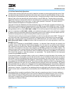
Figure 4-11. Data Cache Debug Tag Register Low (DCDBTRL)
0:12 Reserved
13 UPAR U bit parity
The parity for the U0-U3 bits in the cache line read
by dcread if CCR0[CRPE] = 1, otherwise 0.
14:15 TPAR Tag parity
The parity for the tag bits in the cache line read by
dcread if CCR0[CRPE] = 1, otherwise 0.
16:19 DPAR Data parity
The parity check values for the data bytes in the
word read by dcread if CCR0[CRPE] = 1, other-
wise 0.
20:23 MPAR Modified (dirty) parity
The parity for the modified (dirty) indicators for
each of the four doublewords in the cache line read
by dcread if CCR0[CRPE] = 1, otherwise 0.
24:27 D Dirty Indicators
The “dirty” (modified) indicators for each of the four
doublewords in the cache line read by dcread.
28 U0 U0 Storage Attribute
The U0 storage attribute for the memory page
associated with this cache line read by dcread.
29 U1 U1 Storage Attribute
The U1 storage attribute for the memory page
associated with this cache line read by dcread.
30 U2 U2 Storage Attribute
The U2 storage attribute for the memory page
associated with this cache line read by dcread.
31 U3 U3 Storage Attribute
The U3 storage attribute for the memory page
associated with this cache line read by dcread.
0 23 24 25 27 28 31
TRA
V
TERA
0 12 13 14 15 16 19 20 23 24 27 28 29 30 31
D
U0
U1
U3
U2
UPAR
TPAR
DPAR
MPAR