


User’s Manual
PPC440x5 CPU Core Preliminary
Page 36 of 589
overview.fm.
September 12, 2002
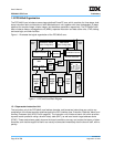
1.4.1 Processor Local Bus (PLB)
There are three independent 128-bit PLB interfaces to the PPC440x5 core. Each of these interfaces includes
a 36-bit address bus and a 128-bit data bus. One PLB interface supports instruction cache reads, while the
other two support data cache reads and writes, respectively. The frequency of each PLB interface can be
independently specified, allowing an IBM CoreConnect system in which the interfaces are not all connected
as part of the same PLB and in which each PLB subsystem operates at its own frequency. Each PLB inter-
face frequency can be configured to any value such that the ratio of the processor core frequency to the PLB
(core:PLB) is n:1, n:2, or n:3, where n is any integer greater than or equal to the denominator of the ratio.
Each of the PLB interfaces supports connection to a PLB subsystem of either 32, 64, or 128 bits. The instruc-
tion and data cache controllers handle any dynamic data bus resizing which is required when the subsystem
data width is less than the 128 bits of the PPC440x5 core PLB interfaces.
The data cache PLB interfaces make requests for 32-byte lines, as well as for 1 - 15 bytes within a 16-byte
(quadword) aligned region. A 16-byte line request is used for quadword APU load operations to caching
inhibited pages, and for quadword APU store operations to caching inhibited, write-through, or “without allo-
cate” pages.
The instruction cache controller makes 32-byte line read requests, and also presents quadword burst read
requests for up to three 32-byte lines (six quadwords), as part of its speculative line fill mechanism.
Each of the PLB interfaces fully supports the address pipelining capabilities of the PLB, and in fact can go
beyond the pipeline depth and minimum latency which the PLB supports. Specifically, each interface
supports up to three pipelined request/acknowledge sequences prior to performing the data transfers associ-
ated with the first request. For the data cache, if each of the requests must themselves be broken into three
separate transactions (for example, for a misaligned doubleword request to a 32-bit PLB slave), then the
interface actually supports up to nine outstanding request/acknowledge sequences prior to the first data
transfer. Furthermore, each PLB interface tolerates a zero-cycle latency between the request and the
address and data acknowledge (that is, the request, address acknowledge, and data acknowledge may all
occur in the same cycle).
1.4.2 Device Control Register (DCR) Interface
The DCR interface provides a mechanism for the PPC440x5 core to setup other on-chip facilities. For
example, programmable resources in an external bus interface unit may be configured for usage with various
memory devices according to their transfer characteristics and address assignments. DCRs are accessed
through the use of the PowerPC mfdcr and mtdcr instructions.
The interface is interlocked with control signals such that it may be connected to peripheral units that may be
clocked at different frequencies from the processor core. The design allows for future expansion of the non-
core facilities without changing the I/O on either the PPC440x5 core or the ASIC peripherals.
The DCR interface also allows the PPC440x5 core to communicate with peripheral devices without using the
PLB interface, thereby avoiding the impact to the primary system bus bandwidth, and without additional
segmentation of the useable address map.
1.4.3 Auxiliary Processor Unit (APU) Port
This interface provides the PPC440x5 core with the flexibility for attaching a tightly-coupled coprocessor-type
macro incorporating instructions which go beyond those provided within the processor core itself. The APU
port provides sufficient functionality for attachment of various coprocessor functions such as a fully-compliant