User’s Manual
PPC440x5 CPU Core Preliminary
Page 246 of 589
debug.fm.
September 12, 2002
8.6.6 Data Address Compare Registers (DAC1–DAC2)
The two DAC registers specify the addresses upon which DAC (and/or DVC) debug events should occur.
Each of the DAC registers can be written from a GPR using mtspr, and can be read into a GPR using mfspr.
8.6.7 Data Value Compare Registers (DVC1–DVC2)
The DVC registers specify the data values upon which DVC debug events should occur. Each of the DVC
registers can be written from a GPR using mtspr, and can be read into a GPR using mfspr.
Figure 8-5. Instruction Address Compare Registers (IAC1–IAC4)
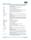
0:29 Instruction Address Compare (IAC) word address
30:31 Reserved
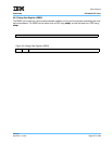
Figure 8-6. Data Address Compare Registers (DAC1–DAC2)
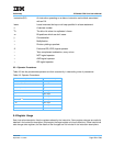
0:31 Data Address Compare (DAC) byte address
Figure 8-7. Data Value Compare Registers (DVC1–DVC2)
0:31 Data value to compare
0 29 30 31
0 31
0 31


