CHAPTER 4 IMAGE PROCESSING SYSTEM
4-4
COPYRIGHT
©
2000 CANON INC. CANON imageRUNNER 600 REV.1 JAN. 2000 PRINTED IN U.S.A.
II . ANALOG IMAGE PROCESSING
A. Outline
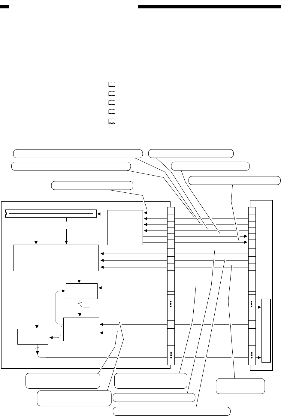
Analog image processing takes place on the CCD PCB, which possesses the following func-
tions:
1. CCD drive Part 2>Chapter 3>1.1
2. CCD output offset correction Part 2>Chapter 3>1.3
3. CCD output gain correction Part 2>Chapter 3>1.3
4. CCD output A/D conversion Part 2>Chapter 3>1.4
5. Real-time AE processing Part 2>Chapter 3>2.5.1
(ABC processing)
Figure 4-201 Functional Block Diagram
CCD
A/D
conversion
Analog signal processing block
1. Gain correction
2. Offset correction
A/D
conversion
Analog image
signal
Digital image signal
Digital image signal
ABC-ON
CCD-ON
CCD-CLK
AD-CLK
AD-LD
AD-DT
R-CLK
HSYNC
CLK-DT
CLK-LD
P-LNG
P-WD
CCD PCB
CCD drive
control
(sync pulse
generation)
Image processing PCB
8
8
Shading correction
Even-numbered pixels
Even-numbered pixels
Odd-numbered
pixels
Odd-numbered
pixels
AE
procession
(ABC circuit)
J1502
J1105
40
46
47
48
34
35
38
39
30
31
40
46
47
48
34
35
38
39
30
31
Communicates timing for CLK-DT reading.
Communicates timing for AD-DT reading.
Data for gain/
offset correction
Main scanning sync signal
Clock, pulses for data reading
Clock pulses for data reading
42
43
13
3
45
37
17
42
43
13
3
45
37
17
When '1', the CCD turns on.
Width of an original (main
scanning direction)
When '1', the ABC circuit
executes AE.
Length of an original (sub
scanning direction)
Sync clock, pulses for the reader
Data for generating sync, pulses for the reader


