


TMP92CZ26A
92CZ26A-97
ZZ12H
1234H
400001H
400000H
800000H
D15 ∼ D0
SRLLB
SRLUB
SRWR
RD
A23 ∼ A0
1CS
busak
busrq
int_xx
SDCLK
DMAC/read
DMAC/write
CPU execution
c
y
cle
Undefined after interrupt
request is asserted until
DMAC read cycle is
started
ZZ34H
CPU execution cycle
2CS
(2) Bus arbitration
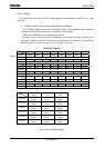
The TMP92CZ26A includes three controllers (DMA controller, LCD controller, SDRAM
controller) that function as bus masters apart from the CPU. These controllers operate
independently and assert a bus request as required. The controller that receives a bus
acknowledgement acts as the bus master. No priorities are assigned to these three
controllers, and bus requests are processed in the order in which they are asserted. Once
one of the controllers owns the bus, bus requests from other controllers are put on hold until
the bus is released again. While one of the controllers is occupying the bus, CPU processing
including non-maskable interrupt requests is also put on hold.
(3) Transfer source and destination memory setting
Either internal or external memory can be set as the source and destination memory or
I/O to be accessed by the DMAC. Even when the MMU is used in external memory, the
addresses to be accessed by the DMAC should be specified using logical addresses. The
DMAC accesses the specified source and destination addresses according to the bus width
and number of waits set in the memory controller and the bank settings made in the MMU.
Although the bus sizing function is supported, the address alignment function is not
supported. Therefore, specify an even-numbered address for transferring 2 bytes and an
address that is an integral multiple of 4 for transferring 4 bytes.
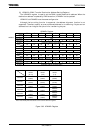
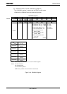
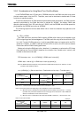
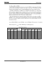
Table 3.6.1 Difference point of address setting between HDMA and micro DMA
Data Length HDMA Micro DMA
1byte No restriction
2byte Even address
Source address
4byte Address in multiples of 4
1byte No restriction
2byte Even address
Destination address
4byte Address in multiples of 4
No restriction
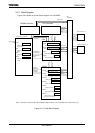
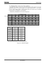
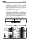
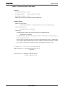
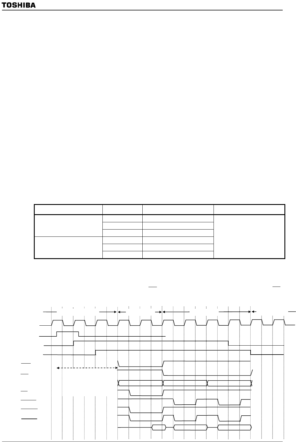
(4) Operation timing
The following diagram shows an example of operation timing for transferring 2 bytes
from 16-bit memory connected with the
2CS area to 8-bit memory connected with the 1CS
area.