


TMP92CZ26A
92CZ26A-696
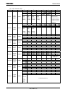
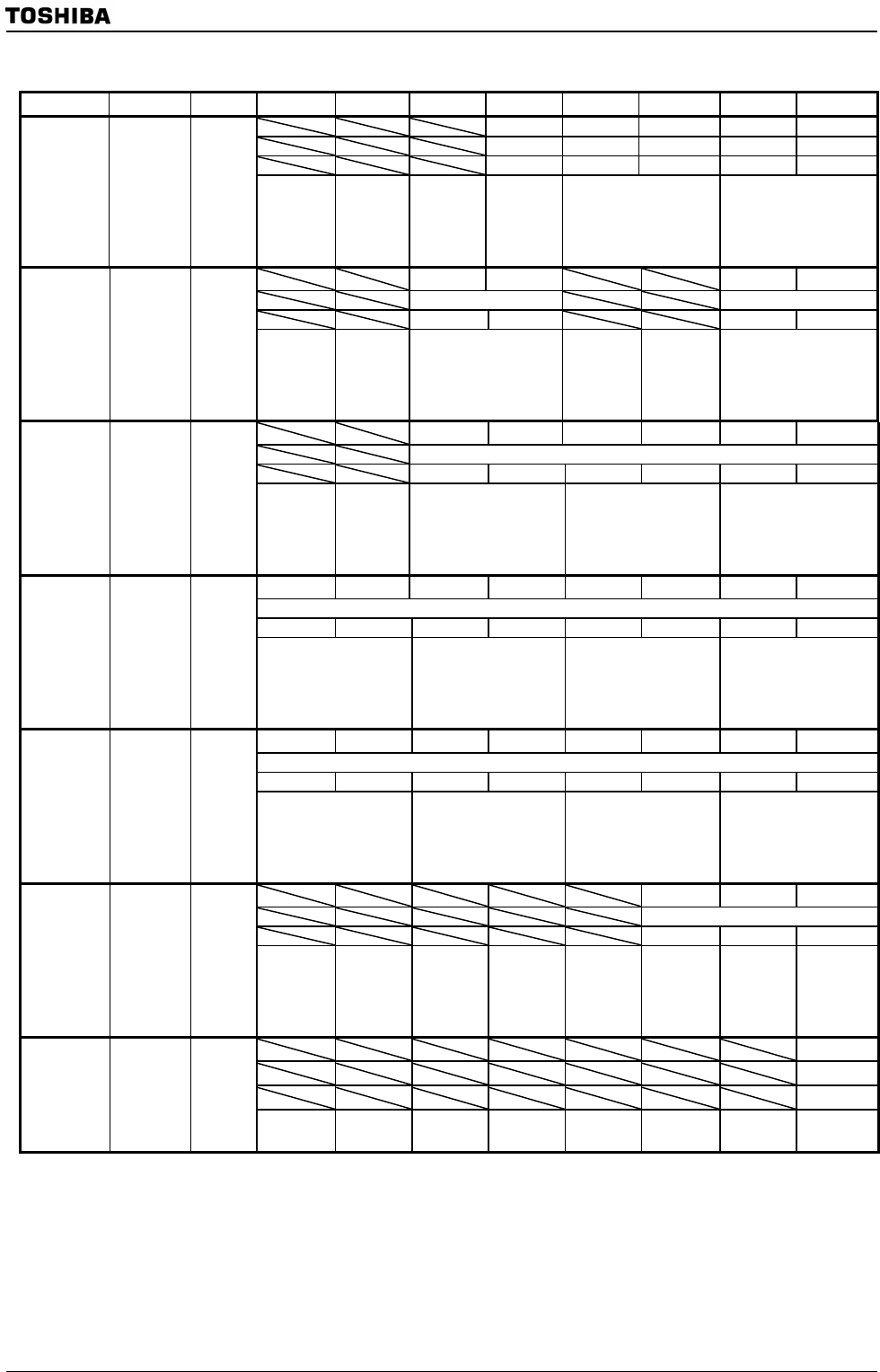
(3) Memory controller (4/4)
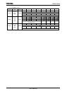
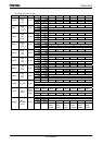
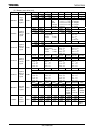
Symbol Name
Address 7 6 5 4 3 2 1 0
OPGE OPWR1 OPWR0 PR1 PR0
R/W
0 0 0 1 0
PMEMCR
Page
ROM
control
register
0166H
ROM
page
access
0: Disable
1: Enable
Wait number on page
00: 1 CLK (n-1-1-1 mode)
01: 2 CLK (n-2-2-2 mode)
10: 3 CLK (n-3-3-3 mode)
11: Reserved
Byte number in a page
00: 64 bytes
01: 32 bytes
10: 16 bytes
11: 8 bytes
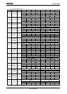
TACSEL1 TACSEL0 TAC1 TAC0
R/W R/W
0 0 0 0
CSTMGC
Adjust for
Timing of
control
signal
0168H
Select area to
change timing
00:CS0 01:CS1
10:CS2 11:CS3
Select delay time(TAC)
00:0 × f
SYS
01:1 × f
SYS
10:2 × f
SYS
11:Reserved
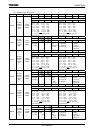
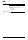
TCWSEL1 TCWSEL0 TCWS1 TCWS0 TCWH1 TCWH0
R/W
0 0 0 0 0 0
WRTMGCRR
Adjust for
Timing of
control
signal
0169H
Select area to
change timing
00:CS0 01:CS1
10:CS2 11:CS3
Select delay time(TCWS)
00:0.5 × f
SYS
01:1.5
× f
SYS
10:2.5
× f
SYS
11:3.5
× f
SYS
Select delay time(TCWH)
00:0.5 × f
SYS
01:1.5
× f
SYS
10:2.5
× f
SYS
11:3.5
× f
SYS
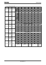
B1TCRS1 B1TCRS0 B1TCRH1 B1TCRH0 B0TCRS1 B0TCRS0 B0TCRH1 B0TCRH0
R/W
0 0 0 0 0 0 0 0
RDTMGCR0
Adjust for
Timing of
control
signal
016AH
Select delay time(TCRS)
00:0.5 × f
SYS
01:1.5
× f
SYS
10:2.5
× f
SYS
11:3.5
× f
SYS
Select delay time(TCRH)
00:0 × f
SYS
01:1
× f
SYS
10:2
× f
SYS
11:3
× f
SYS
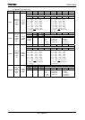
Select delay time(TCRS)
00:0.5 × f
SYS
01:1.5
× f
SYS
10:2.5
× f
SYS
11:3.5
× f
SYS
Select delay time(TCRH)
00:0 × f
SYS
01:1
× f
SYS
10:2
× f
SYS
11:3
× f
SYS
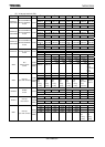
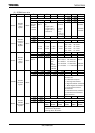
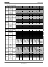
B3TCRS1 B3TCRS0 B3TCRH1 B3TCRH0 B2TCRS1 B2TCRS0 B2TCRH1 B2TCRH0
R/W
0 0 0 0 0 0 0 0
RDTMGCR1
Adjust for
Timing of
control
signal
016BH
Select delay time(TCRS)
00:0.5 × f
SYS
01:1.5
× f
SYS
10:2.5
× f
SYS
11:3.5
× f
SYS
Select delay time(TCRH)
00:0 x× f
SYS
01:1
× f
SYS
10:2
× f
SYS
11:3
× f
SYS
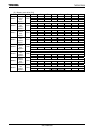
Select delay time(TCRS)
00:0.5 × f
SYS
01:1.5
× f
SYS
10:2.5
× f
SYS
11:3.5
× f
SYS
Select delay time(TCRH)
00:0 × f
SYS
01:1
× f
SYS
10:2
× f
SYS
11:3
× f
SYS
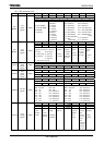
CSDIS ROMLESS VACE
R/W
1 0/1 1/0
BROMCR
Boot Rom
Control
register
016CH
Nand-Flash
Area CS
Output
0:enable
1:disable
Boot
ROM
0: Use
1: No use
Vector
address
0: Disable
1: Enable
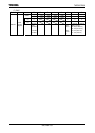
−
R/W
1
RAMCR
RAM
Control
register
016DH
Always
write “1”