TMP92CZ26A
92CZ26A-144
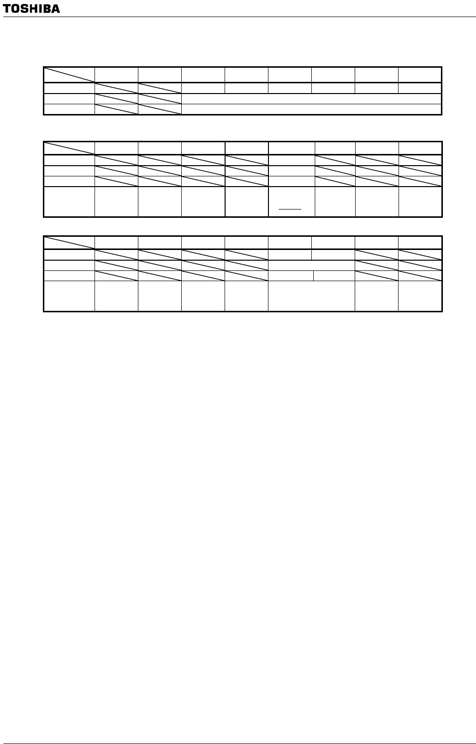
Port G register
7 6 5 4 3 2 1 0
Bit Symbol PG5 PG4 PG3 PG2 PG1 PG0
Read/Write R
After reset Data from external port
Note: Selection of the input channel of AD converter and ADTRG input mode register is enabled by setting AD converter.
Port G Function register
7 6 5 4 3 2 1 0
Bit Symbol PG3F
Read/Write W
After reset 0
Function 0: Input port
or AN3
1:
ADTRG
Port G driver register
7 6 5 4 3 2 1 0
Bit Symbol PG3D PG2D
Read/Write R/W
After reset 1 1
Function Input/Output buffer
drive register for
standby mode
Figure 3.7.30 Register for Port G
Note 1: Read-Modify-Write is prohibited for the registers PGFC.
Note 2: (PG) register is prohibited to access by byte. All the instruction (Arithmetic/ Logical/ Bit operation and rotate/ shift
instruction) access by byte are prohibited. Word access is always needed.
Example: LD wa, (PG) : Using only “a” register data, and cancel “w” register data.
Note 3: Don’t use PG register at the state that mingles Analog input and Digital input.
PG
(0040H)
PGDR
(0090H)
PGFC
(0043H)


