


TMP92CZ26A
92CZ26A-100
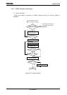
3.6.6 Considerations for Using More Than One Bus Master
In the TMP92CZ26A, the LCD controller, SDRAM controller, and DMA controller may act as
the bus master apart from the CPU. Therefore, care must be exercised to enable each of these
functions to operate smoothly.
To facilitate explanation of DMA operation performed by each bus master, the DMA transfer
operation performed by the DMA controller is defined as “HDMA”, the display RAM read
operation performed by the LCD controller as “LDMA”, and the SDRAM auto refresh operation
performed by the SDRAM controller as “ARDMA”.
The following explains various cases where two or more bus masters may operate at the
same time.
(1) CPU + HDMA
The DMA controller performs DMA transfer (HDMA) after issuing a bus request to the
CPU and getting a bus acknowledgement. The DMA controller may be active while the CPU
is in HALT mode (IDLE2 mode only), in which case HDMA does not interfere with the CPU
operation. However, if HDMA is started while the CPU is active, the CPU cannot execute
instructions while HDMA is being performed.
Before activating the DMA controller, therefore, it is necessary to estimate the CPU stop
time (defined as “t
STOP
(HDMA)”) based on the transfer time, transfer start interval, and
number of channels to be used.
CPU bus stop rate = t
STOP
(HDMA)[s] / HDMA start interval
[s]
HDMA start interval
[s] = HDMA start interrupt period [s]
Note: The HDMA start interval depends on the period of the HDMA start interrupt source. However, it is also
possible to start HDMA by software.
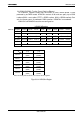
t
STOP
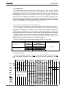
(HDMA) [s] = (Source read time + Destination write time) × Transfer count + α
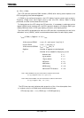
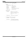
state/byte
Memory Type
Read / Write
Internal RAM
External SDRAM
16-bit bus
External SRAM
16-bit bus
External SRAM
8-bit bus
Read
1 / 4
(Note 1)
Burst 1 / 2
(Note 2)
1 word 6 / 2
(Note 2)
2 / 2
(Note 3)
2 / 1
(Note 3)
Write 1 / 4
Burst 1 / 2
(Note 2)
1 word 3 / 2
(Note 2)
2 / 2
(Note 3)
2 / 1
(Note 3)
Note 1: 2-1-1-1 access. Each consecutive address can be accessed in 1 state.
Note 2: The transfer speed varies depending on the combination of source and destination.
a) When the source or destination is internal RAM or internal I/O (SFR), burst access (6-1-1-1 access)
is possible. Only consecutive addresses on the same page can be accessed in 1 state. Additional 4
states are needed at the end of each burst access.
b) When the source or destination is other than internal RAM or internal I/O, 1-word access is used.
Note 3: In the case of 0 waits
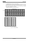
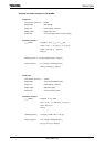
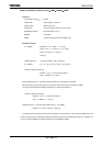
state/byte
I/O Type
Read / Write
I2S NANDF USB SPI
Read
−
2 / 2 2 / 2 2 / 4
Write 2 / 4 2 / 2 2 / 2 2 / 4