


TMP92CZ26A
92CZ26A-219
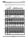
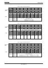
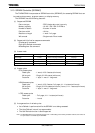
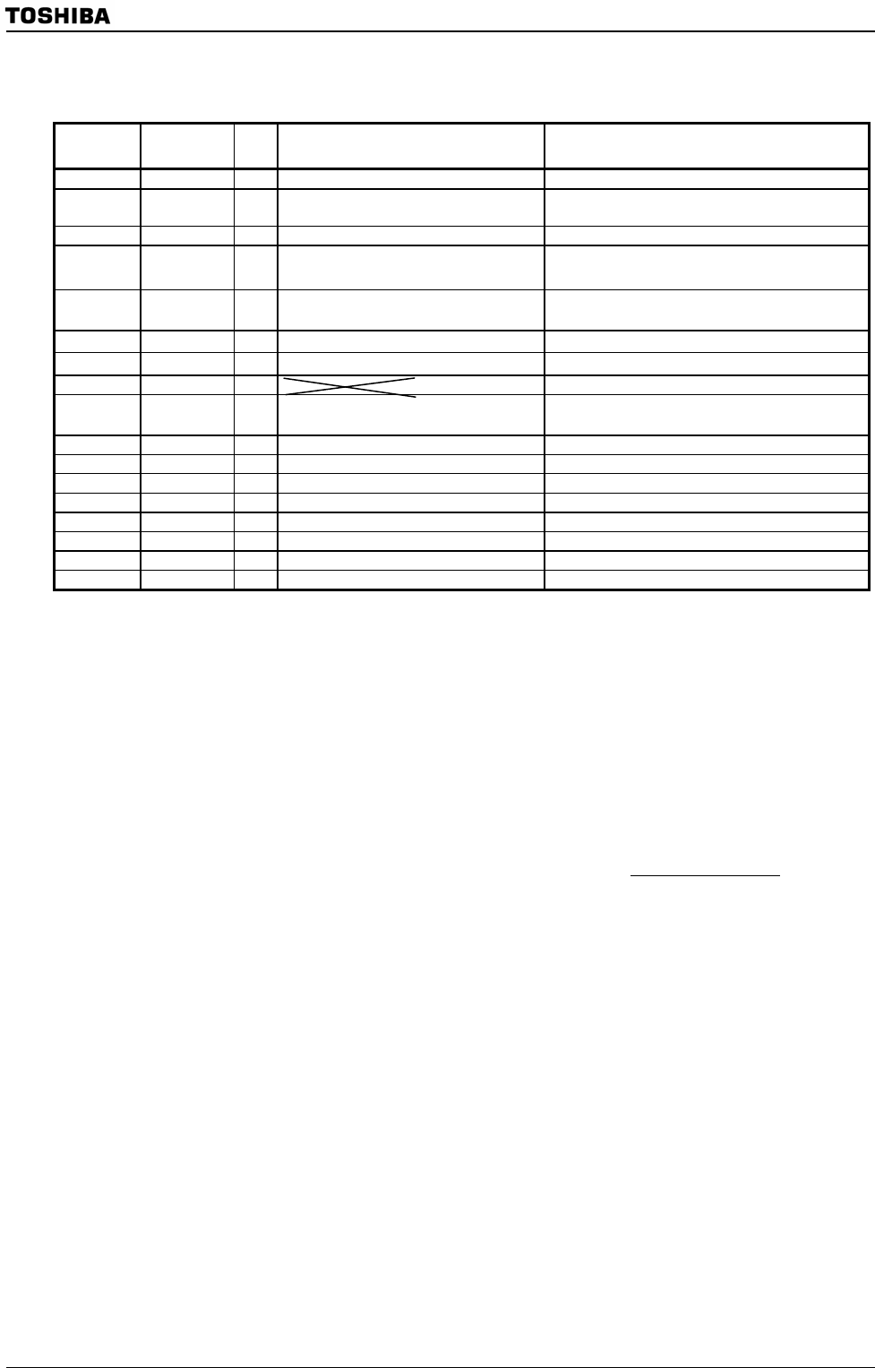
(b) Sub routine (Bank-0 in LOCAL-Y)
Logical
address
Physical
address
No Instruction Comment
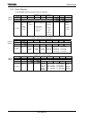
16 org 400000H ;
400000H 000000H 17 ldw (localwy),8001H ; Bank1 in LOCAL-Y is set to write-data for LCD
Display RAM
4000xxH 0000xxH 18 ldw (locally), 8001H ; Bank1 in LOCAL-Y is set as LCD display RAM
19 ldw (localrz), 8001H
; Bank0 in LOCAL-Z is set as read-data
for Character-RAM
20 ld xiy,800000H
; Index address register for read
Character-ROM
21 ld wa,(xiy) ; Read Character-ROM
22 :
; Convert it to display-data
23 ld (localpy), 82H ;
24 ld xix, 400000H
; Index address register for write LCD
Display data
25 ld (xix), bc ; Write LCD Display data
26 : ; Set LCD Controller
27 : ;
28 ld xiz, 400000H ; Set LCD Start address to LCDC
29 ld (lsarcl), xiz ;
30 ld (lcdctl0),01H ; Start LCD Display operation
31 : ;
5000yyH 1000yyH 32 ret ;
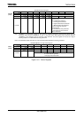
No.17 and No.18 are setting for Bank-1 of LOCAL-Y. In this case, LCD Display data is written to SRAM by CPU.
So, (LOCALWY) and (LOCALLY) should be set to same bank-1.
No.19 is a setting for Bank-0 of LOCAL-Z to read data from character-ROM.
No.20 and No.21 are instructions to read data from character-ROM. When CPU outputs 800000H address, this MMU will
convert and output 000000H address to external address bus: A23 to A0. And /CSZA for NOR-Flash will be asserted
because of logical address is in an area for CS2 at the same time.
By these instructions, CPU can read data from character ROM.
No.23 is an instruction which changes Program bank number in the LOCAL-area. This setting is disabled.
No.24 and No.25 are instructions to write data to SRAM. When CPU outputs 400000H address, this MMU will convert and
output 200000H address to external address bus: A23 to A0. And /CS1 for SRAM will be asserted because of logical
address is in an area for CS1 at the same time.
By these instructions, CPU can write data to SRAM.
No.28 and No.29 are setting to set LCD starting address to LCD Controller. When LCDC outputs 400000H address in
DMA-cycle, this MMU will convert and output 200000H address to external address bus: A23 to A0. And /CS1 for SRAM
will be asserted because of logical address is in an area for CS1 at the same time.
By these instructions, LCDC can read data from SRAM.
No.30 is an instruction to start LCD display operation.