


TMP92CZ26A
92CZ26A-110
3.7 Function of ports
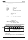
TMP92CZ26A has I/O port pins that are shown in Table 3.7.1 in addition to functioning as
general-purpose I/O ports, these pins are also used by internal CPU and I/O functions.
Table
3.7.2 lists I/O registers and their specifications.
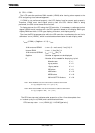
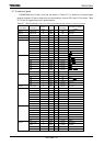
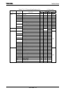
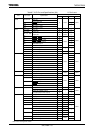
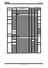
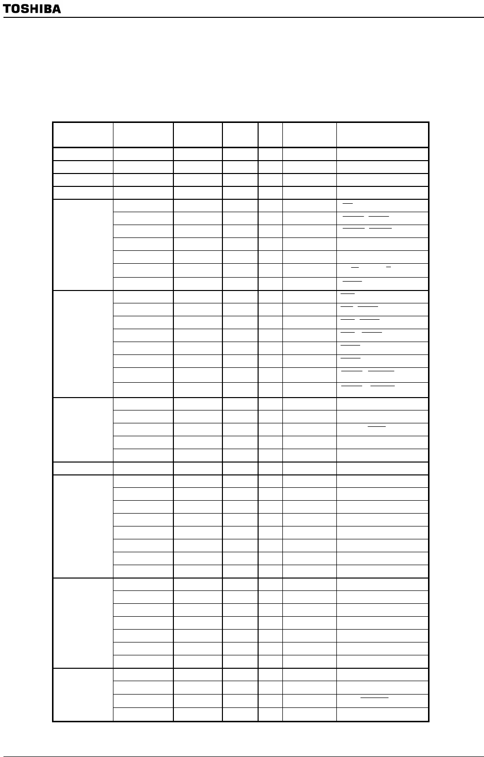
Table 3.7.1 Port Functions (1/3)
(R: PD= with programmable pull-down resistor, U= with pull-up resistor)
Port Name Pin Name
Number of
Pins
I/O R I/O Setting
Pin Name for built-in
function
Port 1 P10 to P17 8 I/O
−
bit D8 to D15
Port 4 P40 to P47 8 Output
−
bit A0 to A7
Port 5 P50 to P57 8 Output
−
bit A8 to A15
Port 6 P60 to P67 8 I/O
−
bit A16 to A23
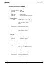
P70 1 Output
−
(Fixed)
RD
P71 1 I/O
−
bit
WRLL
,
NDRE
P72 1 I/O
−
bit
WRLU
,
NDWE
P73 1 I/O
−
bit EA24
P74 1 I/O
−
bit EA25
P75 1 I/O
−
bit
R/
W
, NDR/ B
Port 7
P76 1 I/O
−
bit
WAIT
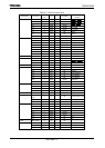
P80 1 Output
−
(Fixed)
0CS
P81 1 Output
−
(Fixed)
1CS
,
SDCS
P82 1 Output
−
(Fixed)
2CS
,
CSZA
P83 1 Output
−
(Fixed)
3CS
,
CSXA
P84 1 Output
−
(Fixed)
CSZB
P85 1 Output
−
(Fixed)
CSZC
P86 1 Output
−
(Fixed)
CSZD , CE0ND
Port 8
P87 1 Output
−
(Fixed)
CSXB , CE1ND
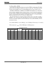
P90 1 I/O
−
bit TXD0
P91 1 I/O
−
bit RXD0
P92 1 I/O
−
bit
SCLK0,
0CTS
P96 1 Input PD (Fixed) INT4, PX
Port 9
P97 1 Input
−
(Fixed) PY
Port A PA0 to PA7 8 Input U (Fixed) KI0 to KI7
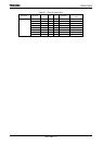
PC0 1 I/O
−
bit INT0
PC1 1 I/O
−
bit INT1, TA0IN
PC2 1 I/O
−
bit INT2
PC3 1 I/O
−
bit INT3, TA2IN
PC4 1 I/O
−
bit EA26
PC5 1 I/O
−
bit EA27
PC6 1 I/O
−
bit EA28
Port C
PC7 1 I/O
−
bit KO8
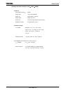
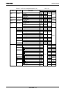
PF0 1 I/O
−
bit I2S0CKO
PF1 1 I/O
−
bit I2S0DO
PF2 1 I/O
−
bit I2S0WS
PF3 1 I/O
−
bit I2S1CKO
PF4 1 I/O
−
bit I2S1DO
PF5 1 I/O
−
bit I2S1WS
Port F
PF7 1 Output
−
(Fixed) SDCLK
PG0 to PG1 2 Input
−
(Fixed) AN0 to AN1
PG2 1 Input
−
(Fixed) AN2, MX
PG3 1 Input
−
(Fixed)
AN3,
ADTRG
, MY
Port G
PG4 to PG5 2 Input
−
(Fixed) AN4 to AN5