


TMP92CZ26A
92CZ26A-26
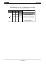
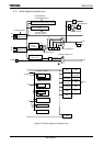
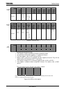
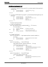
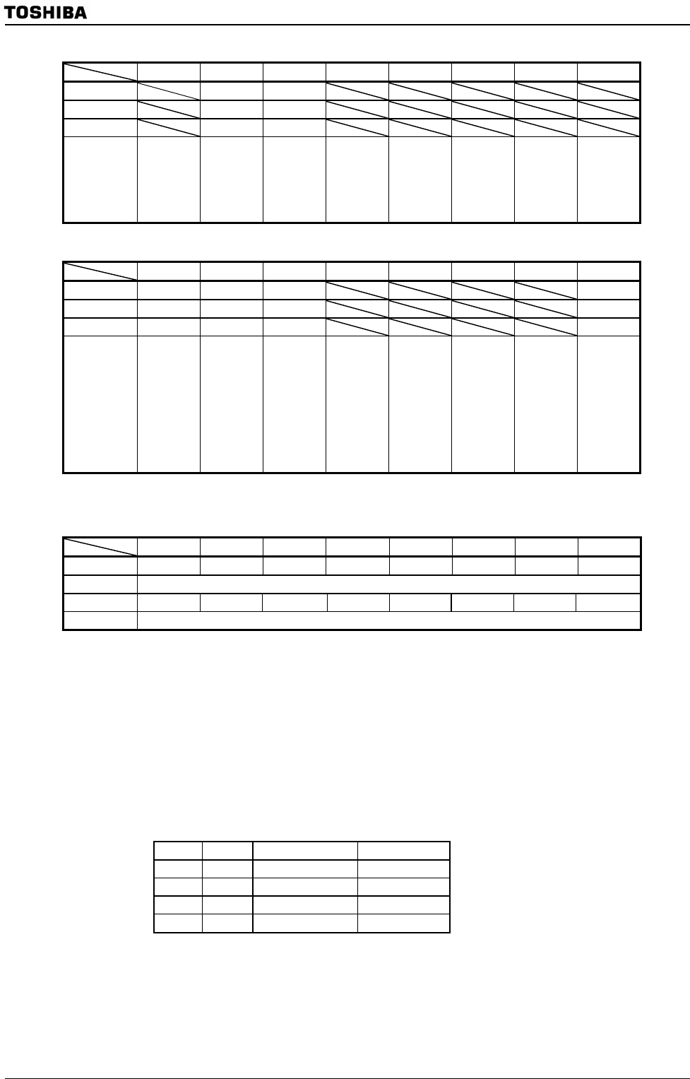
7 6 5 4 3 2 1 0
bit symbol FCSEL LUPFG
Read/Write R/W R
After reset 0 0
Function
Select
fc-clock
0 : f
OSCH
1 : f
PLL
Lock-up
timer
Status flag
0 : not end
1 : end
Note: Be carefull that logic of PLLCR0<LUPFG> is different from 900/L1’s DFM.
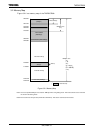
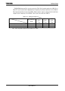
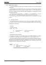
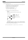
7 6 5 4 3 2 1 0
bit symbol PLL0 PLL1 LUPSEL
PLLTIMES
Read/Write R/W R/W R/W R/W
After reset 0 0 0 0
Function
PLL0 for
CPU
0: Off
1: On
PLL1 for
USB
0: Off
1: On
Select
stage of
Lock up
counter
0: 12 stage
(for PLL0)
1:13 stage
(for PLL1)
Select the
number of
PLL
0: ×12
1: ×16
Figure 3.3.5 SFR for PLL
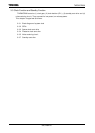
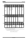
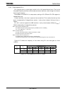
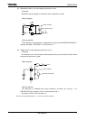
7 6 5 4 3 2 1 0
bit symbol Px7D Px6D Px5D Px4D Px3D Px2D Px1D Px0D
Read/Write R/W
After reset 1 1 1 1 1 1 1 1
Function Output/Input buffer drive-register for standby-mode
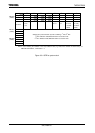
(Purpose and method of using)
• This register is used to set each pin-status at stand-by mode.
• All ports have this format’s register. (“x” means port-name.)
• For each register, refer to 3.5 Function of Ports.
• Before “HALT” instruction is executed, set each register pin-status. They will be
effective after CPU executes “HALT” instruction.
• This register is effective in all stand-by modes (IDLE2, IDLE1 or STOP).
• This register is effective when using PMC function. For details, refer to PMC
section.
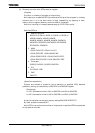
The truth table to control Output/Input-buffer is below.
OE PxnD Output buffer Input buffer
0 0 OFF OFF
0 1 OFF ON
1 0 OFF OFF
1 1 ON OFF
Note1: OE means an output enable signal before stand-by mode. Basically, PxCR is used as OE.
Note2: “n” in PxnD means bit-number of PORTx.
Figure 3.3.6 SFR for drive register
PLLCR0
(10E8H)
PLLCR1
(10E9H)
PxDR
(xxxxH)