


TMP92CZ26A
92CZ26A-106
(4) CPU + LDMA+ ARDMA + HDMA
This is a case in which all the bus masters are active at the same time.
Since the LCD display function cannot work properly if the LCD controller cannot
perform LDMA properly, the priorities among the four bus masters should be set in the
order of LDMA > ARDMA > HDMA > CPU.
Before calculating the CPU bus stop rate, the conditions for proper LCD display shall be
considered first.
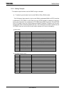
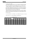
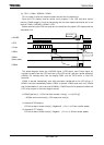
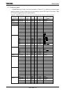
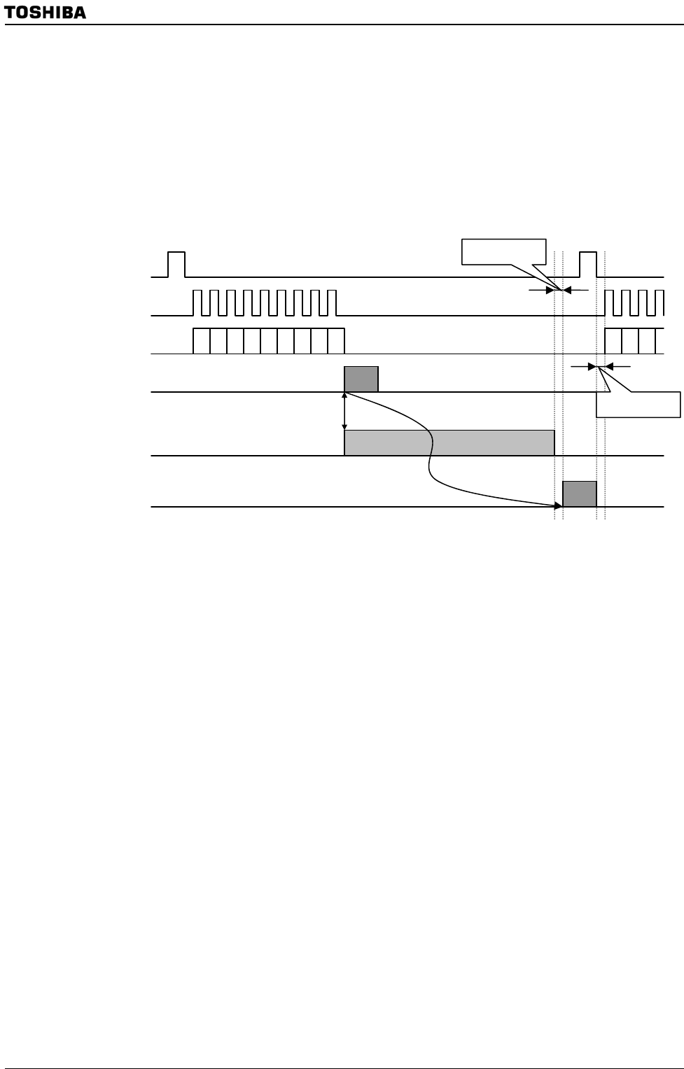
The above diagram shows the LHSYNC signal, LCP0 signal, and LD-bus signal for
transferring data from the LCD controller to the LCD driver, and the transfer operation
(LDMA1) for reading data from the display RAM into the FIFO buffer in the LCD
controller.
LDMA is started immediately after data has been transferred to the LCD driver. If
HDMA is started immediately before LDMA1 is started, LDMA must wait until HDMA
has finished before it can be started (LDMA2). LDMA2 must finish operation before the
LCD driver output for the next stage is started.
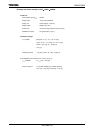
LHSYNC
[period: s] − LCD driver data transfer time [s] − t
STOP
(LCD) [s]
= HDMA continuous time [s] + CPU operation time [s]
In the case of STN display
LCD driver data transfer time [s] = SegNum/8 (1/f
SYS
) × (LD bus transfer speed)
In the case of TFT display
LCD driver data transfer time [s] = SegNum (1/ f
SYS
) × (LD bus transfer speed)
LHSYNC
LCP0
LD-bus
LDMA1
HDM
A
(Worst case)
LDMA2
Setup time 1
Setup time 2