


TMP92CZ26A
92CZ26A-509
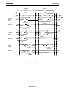
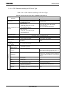
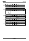
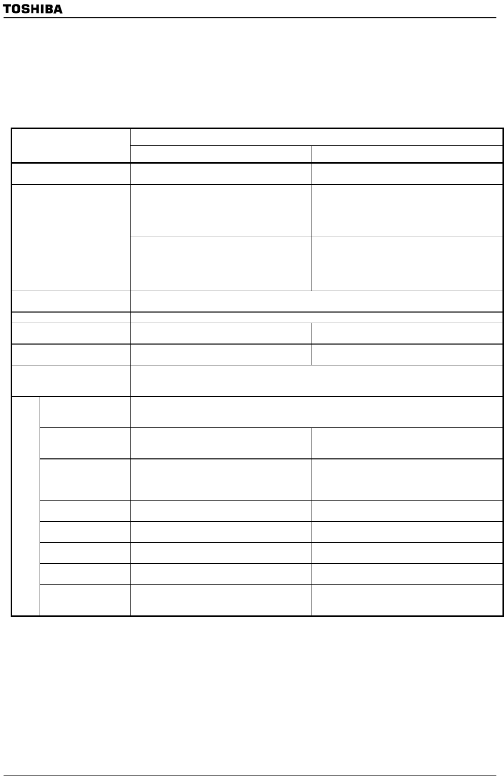
3.19.1 LCDC Features according to LCD Driver Type
Table 3.19.1 LCDC Features according to LCD Driver Type
(This table assumes the connection with a TOSHIBA-made LCD driver.)
Shift Register Type
LCD Driver
TFT STN
Display colors 256/4096/65536/262144/16777216 colors
Monochrome, 4/16/64 grayscale levels
256/4096 colors
For 65536 colors or less
Rows (Commons):
64, 96, 128, 160, 200, 240, 320, 480
Columns (Segments):
64, 128, 160, 240, 320, 640
Rows (Commons):
64, 96, 120, 128, 160, 200, 240, 320, 480
Columns (Segments):
64, 120, 128, 160, 240, 320, 480, 640
Number of pixels that can be
displayed
For 65536 colors or more
Rows (Commons):
64, 96, 128, 160, 200, 240, 320, 480
Columns (Segments):
64, 128, 160, 240, 320
–
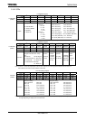
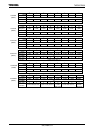
Data rotation function
Horizontal flip, vertical flip, horizontal and vertical flip, 90-degree rotation
(supported for QVGA size, 65536 colors only)
PIP function support A sub window can be inserted.
Source data bus width
(SRAM, SDRAM)
16 bits (32 bits: internal RAM) 16 bits (32 bits: internal RAM)
Destination data bus width
(LCD driver)
8 to 24 bits 8 bits
Maximum transfer rate
(VRAM read)
(at f
SYS
= 80 MHz)
4.17 ns/byte at internal RAM
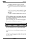
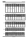
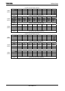
LCD driver data bus:
LD23 to LD0 pins
To be connected to LCD driver data bus.
8-bit mode: LD7 to LD0
TFT mode: LD23 to LD0
LCP0 pin
Data shift clock for TFT source driver Shift clock pulse output pin 0. To be connected to
column driver’s CP pin. The LCD driver latches the
data bus value on the falling edge of this pin.
LHSYNC pin
Vertical shift clock for TFT gate driver Latch pulse output pin. To be connected to the LCD
driver’s LP pin. The display data in the LCD driver’s
output line register is updated on the rising edge of
this pin.
LLOAD pin
Enable signal for TFT source driver to load data
to TFT panel
N/A
LGOE0 to LGOE2
pins
Adjustment signal for TFT gate driver’s gate
control signal
N/A
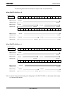
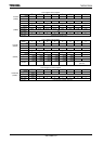
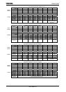
LFR pin
LCD alternate signal output pin. To be connected
to column/row driver’s FR pin.
LCD alternate signal output pin. To be connected to
column/row driver’s FR pin.
LVSYNC pin
This signal indicates the start of shift clock
capture by TFT gate driver.
Frequency that sets LCD refresh rate
External Pins
LDIV pin
This signal indicates the inversion of data. To be
connected to TFT source driver having the data
inversion function.
N/A