TMP92CZ26A
92CZ26A-535
4. LGOE0 to LGOE2 Signals
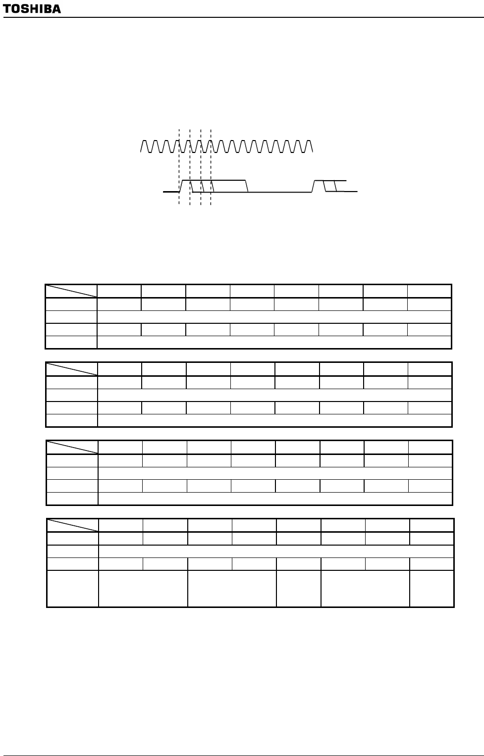
The LCDC has three signals (LGOE0 to LGOE2) that can be controlled like the
LHSYNC signal. For these signals, the enable width, delay time, and phase timing can
be adjusted as shown below.
7 6 5 4 3 2 1 0
bit Symbol O0W7 O0W6 O0W5 O0W4 O0W3 O0W2 O0W1 O0W0
Read/Write W
After reset 0 0 0 0 0 0 0 0
Function LGOE0 width (bits 7-0)
7 6 5 4 3 2 1 0
bit Symbol O1W7 O1W6 O1W5 O1W4 O1W3 O1W2 O1W1 O1W0
Read/Write W
After reset 0 0 0 0 0 0 0 0
Function LGOE1 width (bits 7-0)
7 6 5 4 3 2 1 0
bit Symbol O2W7 O2W6 O2W5 O2W4 O2W3 O2W2 O2W1 O2W0
Read/Write W
After reset 0 0 0 0 0 0 0 0
Function LGOE2 width (bits 7-0)
7 6 5 4 3 2 1 0
bit Symbol O2W9 O2W8 O1W9 O1W8 O0W8 LDW9 LDW8 HSW8
Read/Write W
After reset 0 0 0 0 0 0 0 0
Function
LGOE2 width (bits 9-8) LGOE1 width (bits 9-8) LGOE0
width
(bit 8)
LLOAD width (bits 9-8) LHSYNC
width
(bit 8)
LCP0
Signal Name
LGOE0 signal
LGOE1 signal
LGOE2 signal
High width setting
LGOE0: LCP0 clock = 1, 2, 3 … 512 pulses
LGOE1: LCP0 clock = 1, 2, 3 … 1024 pulses
LGOE2: LCP0 clock = 1, 2, 3 … 1024 pulses
LCDHO0W
(
0296H
)
LCDHO1W
(
0297H
)
LCDHO2W
(
0298H
)
LCDHWB8
(
0299H
)


