


TMP92CZ26A
92CZ26A-76
3.5.3 Interrupt Controller Operation
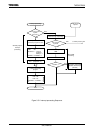
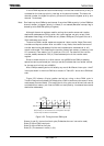
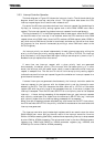
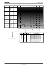
The block diagram in Figure 3.5.3 shows the interrupt circuits. The left-hand side of the
diagram shows the interrupt controller circuit. The right-hand side shows the CPU
interrupt request signal circuit and the halt release circuit.
For each of the 59 interrupts channels there is an interrupt request flag (consisting of a
flip-flop), an interrupt priority setting register and a micro DMA /HDMA start vector
register. The interrupt request flag latches interrupt requests from the peripherals.
The flag is cleared to “0” in the following cases: when a reset occurs, when the CPU reads
the channel vector of an interrupt it has received, when the CPU receives a micro DMA
request (when micro DMA is set), when the CPU receives a HDMA request (when HDMA is
set), when a micro DMA burst transfer is terminated, and when an instruction that clears
the interrupt for that channel is executed (by writing a micro DMA start vector to the
INTCLR register).
An interrupt priority can be set independently for each interrupt source by writing the
priority to the interrupt priority setting register (e.g., INTE0 or INTE12). Six interrupt
priorities levels (1 to 6) are provided. Setting an interrupt source’s priority level to 0 (or 7)
disables interrupt requests from that source.
If more than one interrupt request with a given priority level are generated
simultaneously, the default priority (The interrupt with the lowest priority or, in other
words, the interrupt with the lowest vector value) is used to determine which interrupt
request is accepted first. The 3rd and 7th bits of the interrupt priority setting register
indicate the state of the interrupt request flag and thus whether an interrupt request for a
given channel has occurred.
If several interrupts are generated simultaneously, the interrupt controller sends the
interrupt request for the interrupt with the highest priority and the interrupt’s vector
address to the CPU. The CPU compares the mask value set in <IFF2:0> of the status
register (SR) with the priority level of the requested interrupt; if the latter is higher, the
interrupt is accepted. Then the CPU sets SR<IFF2:0> to the priority level of the accepted
interrupt + 1. Hence, during processing of the accepted interrupt, new interrupt requests
with a priority value equal to or higher than the value set in SR<IFF2:0> (e.g., interrupts
with a priority higher than the interrupt being processed) will be accepted.
When interrupt processing has been completed (e.g., after execution of a RETI instruction),
the CPU restores to SR<IFF2:0> the priority value which was saved on the stack before the
interrupt was generated.
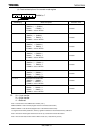
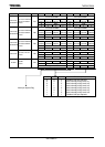
The interrupt controller also includes eight registers which are used to store the micro
DMA /HDMA start vector. Writing the start vector of the interrupt source for the micro
DMA or /HDMA processing (See Table), enables the corresponding interrupt to be processed
by micro DMA or HDMA processing. The values must be set in the micro DMA parameter
registers (e.g., DMAS and DMAD) or HDMA parameter registers (e.g., HDMAS, and
HDMAD) prior to micro DMA or HDMA processing.