


TMP92CZ26A
92CZ26A-406
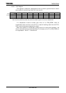
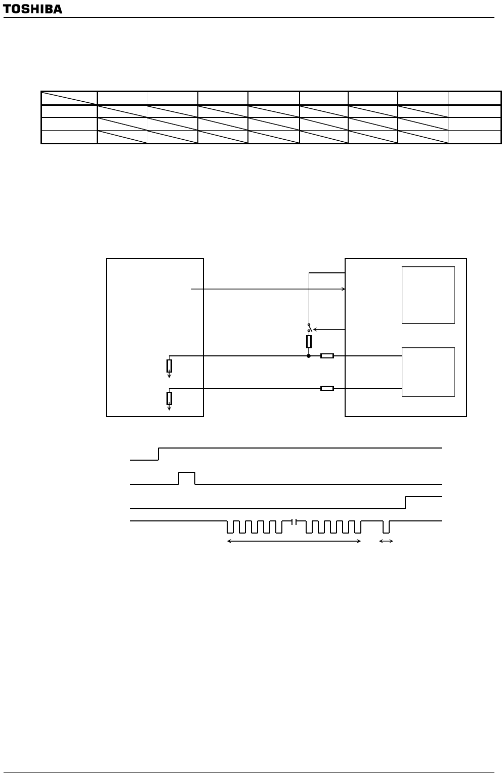
3.16.3.27 USBREADY Register
This register informs finishing writing data to descriptor RAM on UDC.
After assigned data to descriptor RAM, write “0” to bit0.
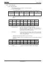
7 6 5 4 3 2 1 0
bit Symbol USBREADY
Read/Write R/W
After reset 0
USBREADY (Bit0)
0: Writing to descriptor RAM was finished.
1: Writing to descriptor RAM is enable.
(However, when during connecting to host, writing to descriptor RAM is prohibited.)
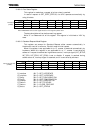
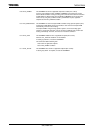
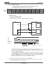
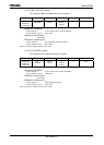
Detect level of VDD signal from USB cable, and execute initialize sequence. In this
case, UDC disable detecting USB_RESET signal until USBREADY register is written
“0” after released USB_RESET.
If pull-up resister on D+ signal is controlled by using control signal, when pull-up
resister is connected to host in OFF condition, this condition is equivalent condition
with USB_RESET signal by pull-down resister in host side. Therefore UDC isn’t
detected in USB_RESET until write “0” to USBREADY register
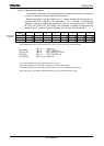
Note1: Pull-up resister and control switch are needed at external of TMP92CZ26A.
Note2: Above setting is example when communication. It is needed special circuit for prevent flow current at
connector connect detection , no-use, no connection.
USBREAD
Y
(07E6H)
VDD
Po
r
tXX
(Pull-up on/off)
INTXX
Write si
g
nal
Descriptor RAM access
Device ID RAM
Re
g
ister in USB
USBREADY registera access
GND
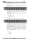
15 kΩ
15 kΩ
USB host
VCC
VSS
PortXX
D+
D−
CPU
UDC
R2
R3
R1 = 1.5 k
Ω
TMP92CZ26A