


TMP92CZ26A
92CZ26A-241
The
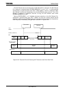
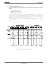
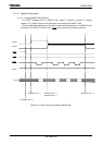
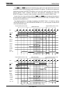
NDRE and NDWE signals are explained next. Write and read operations to and from
the NAND Flash are performed through the ND0FDTR register. The actual write operation
completes not when the ND0FDTR register is written to but when the data is written to the
external NAND Flash. Likewise, the actual read operation completes not when the
ND0FDTR register is read but when the data is read from the external NAND Flash.
At this time, the Low and High widths of
NDRE and NDWE can be adjusted according to
the CPU operating speed (f
SYS
) and the access time of the NAND Flash. (For details, refer to
the electrical characteristics.)
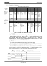
The following shows an example of accessing the NAND Flash in 6 clocks by setting
NDFMCR0<SPLW1:0>=2 and NDFMCR0<SPHW1:0>=2. (In write cycles, the data drive
time also becomes longer.)
Figure 3.11.3 Read/Write Access to NAND Flash
FF1234H
IN (Program)
001FF0H FF1238H
IN
(
Pr
og
r
a
m
)
OUT (NAND Flash)
Program Memory Read (1 wait)
NAND Flash Write
Program Memory Read (1 wait)
2clk
2clk
f
SYS
NDALE
NDRE
NDWE
NDR/B
D15
∼ D0
A
23∼A0
2CS
SRWR
FF1234H
IN
(
Pro
g
ram
)
001FF0H
FF1238H
IN
(
Pro
g
ram
)
IN
(
NAND Flash
)
Program Memory Read (1wait)
NAND Flash Read
Pro
g
ram Memor
y
Read
(
1 wait
)
NDCLE
2clk
2clk
RD
f
SYS
NDALE
NDRE
NDWE
NDR/B
D15
∼ D0
A
23∼A0
2CS
SRWR
NDCLE
RD
NDCE
NDCE