


TMP92CZ26A
92CZ26A-21
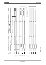
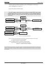
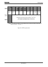
The clock operating modes are as follows: (a) PLL-OFF Mode (X1, X2 pins only),
(b) PLL-ON Mode (X1, X2, and PLL).
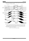
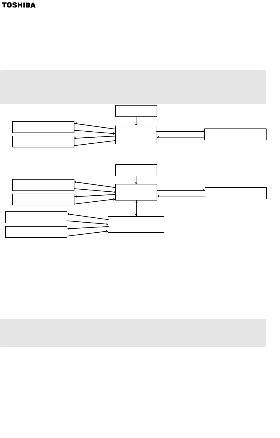
Figure 3.3.1 shows a transition figure.
Reset
(f
OSCH
/16)
release Reset
instruction
interrupt
STOP mode
(Stops all circuits)
PLL-OFF mode
(f
OSCH
/gear value)
IDLE2 mode
(I/O operate)
IDLE1 mode
(Operate only oscillator)
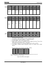
(a) PLL-OFF mode transition figure
(b) PLL-OFF , PLL-ON mode transition figure
PLL-ON mode
((12 or 16)×f
OSCH
/gear value)
Reset
(f
OSCH
/16)
release Reset
PLL-OFF mode
(f
OSCH
/gear value)
IDLE2 mode
(I/O operate)
IDLE1 mode
(Operate only oscillator)
IDLE2 mode
(I/O operate)
IDLE1 mode
(Operate only oscillator)
instruction
instruction
interrupt
interrupt
instruction
instruction
interrupt
interrupt
instruction
instruction
interrupt
interrupt
instruction
interrupt
STOP mode
(Stops all circuits)
Instruction (Note)
Note 1: If you shift from PLL-ON mode to PLL-OFF mode, execute following setting in the same order.
(1) Change CPU clock (Set “0” to PLLCR0<FCSEL>)
(2) Stop PLL circuit (Set “0” to PLLCR1<PLLON>)
Note 2: It’s prohibited to shift from PLL-ON mode to STOP mode directly.
You should set PLL-OFF mode once, and then shift to STOP mode.
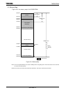
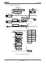
Figure 3.3.1 System clock block diagram
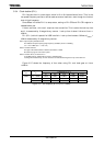
The clock frequency input from the X1 and X2 pins is called fOSCH and the clock
frequency input from the XT1 and XT2 pins is called fs. The clock frequency selected by
SYSCR1<GEAR2:0> is called the system clock fSYS. And one cycle of fSYS is defined to
as one state.
The clock frequency input from the X1 and X2 pins is called f
OSCH
and the clock frequency input from the XT1 and XT2 pins is
called fs. The clock frequency selected by SYSCR1<GEAR2:0> is called the system clock f
SYS
. And one cycle of f
SYS
is defined
to as one state.