


TMP92CZ26A
92CZ26A-595
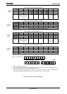
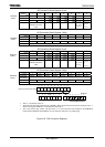
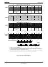
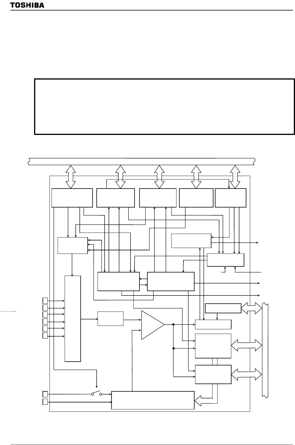
3.23 Analog-Digital Converter (ADC)
This LSI has a 6-channel, multiplexed-input, 10-bit successive-approximation Analog-Digital
converter (ADC).
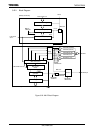
Figure 3.23.1 shows a block diagram of the AD converter.
The 6-analog input channels (AN0-AN5) can be used as general-purpose inputs.
Note1: Ensure that the AD converter has halted before executing HALT instruction to place the
TMP92CZ26A in IDLE2, IDLE1, STOP or PCM mode to reduce power consumption current.
Otherwise, the TMP92CZ26A might go into a standby mode while the internal analog
comparator is still enable state.
Note2: The power consumption current is reduced by setting ADMOD1<DACON> to “0” in the ADC
has been stopped.
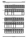
Figure 3.23.1 ADC Block Diagram
A
D Monitor function interrupt
INTADM
Complete interrupt AD
INTADHP
Normal AD Conversion
complete interrupt
INTAD
Comparator
VREFH
VREFL
Sample
Hold
ADMOD1
Scan
re
p
eat
BusyEnd
Start
+
−
Internal data bus
Channel
selection
control circuit
A
/ D Conversion
Result Register
ADREG0L~5L
ADREG0H~5H
D/A Converter
Normal AD
Converter Control
Circuit
ADMOD0 ADMOD2 ADMOD3
High-Priority AD
Converter Control
End
Compare register
1 and 2
AD Monitor
Function control
Busy
AD start control
ADMOD4/5
TRMB/ I2S
A
DS
HTSEL/HHTRGE
ITM/LAT
VREF
TSEL/HTRGE
Start
A
DTRG
AN5 (PG5)
AN4 (PG4)
ADTRG, AN3 (PG3)
AN2 (PG2)
AN1 (PG1)
AN0 (PG0)
Compare circuit
1&2
High-Priority AD
Conversion
Result Register
ADREGSPH/L
Internal data bus
Multiplexer