


TMP92CZ26A
92CZ26A-640
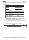
4. Electrical Characteristics (Tentative)
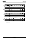
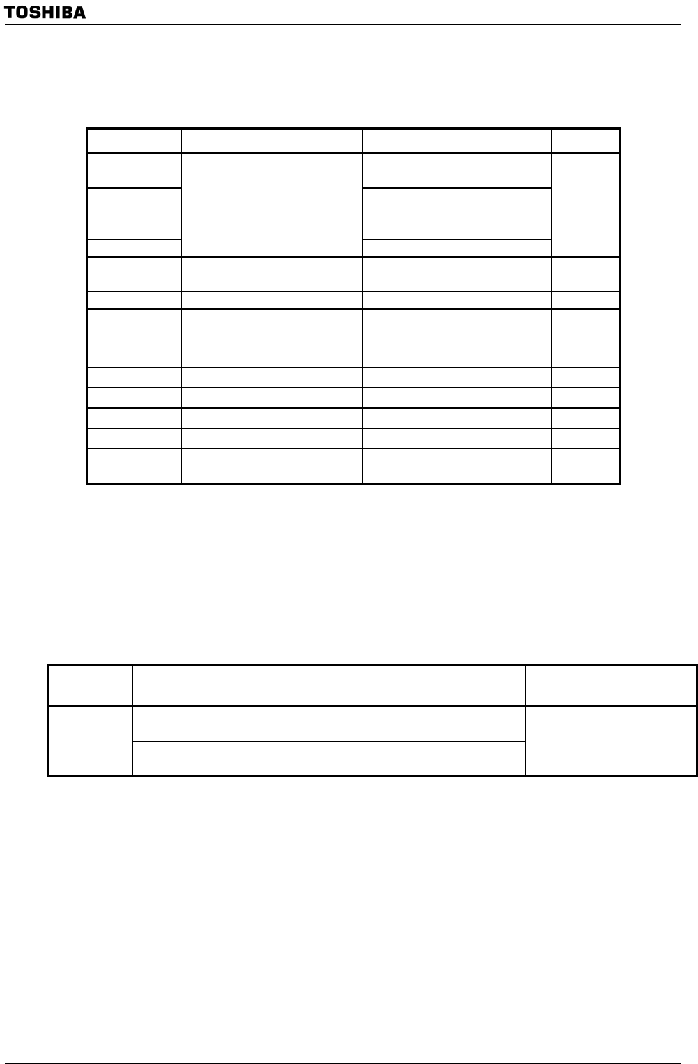
4.1 Maximum Ratings
Symbol Contents Rating Unit
DVCC3A
DVCC3B
-0.3 to 3.9
DVCC1A
DVCC1B
DVCC1C
-0.3 to 3.0
AVCC
Power Supply Voltage
-0.3 to 3.9
V
V
IN
Input Voltage
-0.3 DVCC3A/3B+0.3 (Note1)
-0.3 to AVCC + 0.3 (Note2)
V
IOL Output Current (1pin) 15 mA
IOH Output Current (1pin) -15 mA
Σ
IOL
Output Current (total) 80 mA
Σ
IOH
Output Current (total) -50 mA
P
D
Power Dissipation (Ta = 85°C) 600 mW
T
SOLDER
Soldering Temperature (10s) 260 °C
T
STG
Storage Temperature -65 to 150 °C
T
OPR
Operation Temperature -0 to 70 °C
T
OPR
Operation Temperature
(80MHz)
-0 to 50 °C
Note1: If setting it, don’t exceed the Maximum Ratings of DVCC3A (PV port and PW port are DVCC3B).
Note2: In PG0 to PG5, P96,P97,VREFH,VREFL maximum ratings for AVCC is applied.
Note3: The maximum ratings are rated values that must not be exceeded during operation, even for an instant. Any
one of the ratings must not be exceeded. If any maximum rating is exceeded, a device may break down or its
performance may be degraded, causing it to catch fire or explode resulting in injury to the user. Thus, when
designing products that include this device, ensure that no maximum rating value will ever be exceeded.
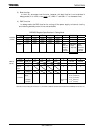
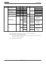
Point of note about solderability of lead free products (attach “G” to package name)
Test
parameter
Test condition Note
Solder bath temperature = 230°C, Dipping time = 5 seconds
The number of times = one, Use of R-type flux
Solderability
Solder bath temperature =245°C, Dipping time = 5 seconds
The number of times = one, Use of R-type flux (use of lead free)
Pass:
solderability rate until forming
≥ 95%