


TMP92CZ26A
92CZ26A-224
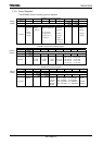
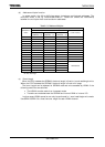
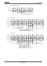
(b) Address multiplex function
In access cycles, the A0 to A15 pins output low/column multiplexed addresses. The
multiplex width is set by SDACR<SMUXW1:0>.
Table3.10.2 shows the relationship
between the multiplex width and low/column addresses.
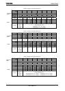
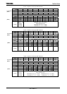
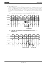
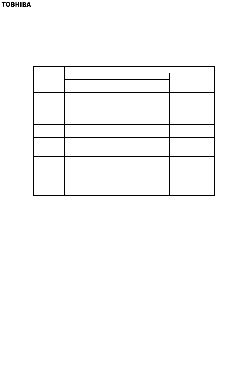
Table3.10.2 Address Multiplex
SDRAM Access Cycle Address
Row Address
92CZ26A Pin
Name
Type A
<SMUXW> = 00
Type B
<SMUXW> = 01
Type C
<SMUXW> = 10
Column Address
A0 A9 A10 A11 A1
A1 A10 A11 A12 A2
A2 A11 A12 A13 A3
A3 A12 A13 A14 A4
A4 A13 A14 A15 A5
A5 A14 A15 A16 A6
A6 A15 A16 A17 A7
A7 A16 A17 A18 A8
A8 A17 A18 A19 A9
A9 A18 A19 A20 A10
A10 A19 A20 A21 AP *
A11 A20 A21 A22
A12 A21 A22 A23
A13 A22 A23 EA24
A14 A23 EA24 EA25
A15 EA24 EA25 EA26
Row Address
*AP: Auto Precharge
(c) Burst length
When the CPU accesses the SDRAM, the burst length is fixed to 1-word read/single write.
When the LCDC accesses the SDRAM, the burst length is fixed to full page.
The burst length can be selected for SDRAM read and write accesses by HDMA if the
following conditions are satisfied:
• The HDMA transfer mode is an increment mode.
• Transfers are made between the SDRAM and internal RAM or internal I/O.
In other cases, HDMA operation can only be performed in 1-word read/single write mode.
Use SDBLS<SDBL5:0> to set the burst length for each HDMA channel.