


TMP92CZ26A
92CZ26A-132
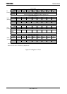
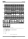
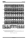
Port 9 register
7 6 5 4 3 2 1 0
bit Symbol P97 P96 P92 P91 P90
Read/Write R R/W
After reset
Data from external
port
Data from external port (Output
latch register is set to “1”)
Port 9 control register
7 6 5 4 3 2 1 0
bit Symbol P92C P91C P90C
Read/Write W
After reset 0 0 0
Function Refer to following table
Port 9 function register
7 6 5 4 3 2 1 0
bit Symbol P96F P92F P90F
Read/Write W W W
After reset 0 0 0
Function
0: Input
port
1: INT4
Refer to
following
table
Refer to
following
table
Port 9 Function registers 2
7 6 5 4 3 2 1 0
bit Symbol − − P90F2
Read/Write W W W
After reset 0 0 0
Function
Always
write “0”
Always
write “0”
0:CMOS
1:
open-drain
Port 9 drive register
7 6 5 4 3 2 1 0
bit Symbol P97D P96D P92D P91D P90D
Read/Write R/W R/W
After reset 1 1 1 1 1
Function Input/Output buffer drive register for standby mode
Note 1: Read-modify-write is prohibited for P9CR, P9FC and P9FC2.
Note 2: When setting P96 pin to INT4 input, set P9DR<P96D> to “0” (prohibit input), and when driving P96 pin to “0”, execute
HALT instruction. This setting generates INT4 inside. If don’t using external interrupt in HALT condition, set like an
interrupt don’t generated. (e.g. change port setting)
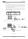
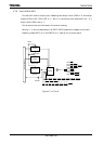
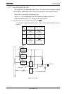
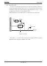
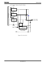
Figure 3.7.17 Register for Port 9
P9FC
(0027H)
P9
(0024H)
P9CR
(0026H)
P9FC2
(0025H)
P9DR
(0089H)
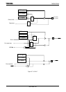
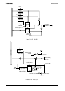
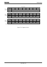
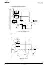
<P90C>
<P90F>
0 1
0 Input port Output port
1
Don’t
setting
TXD0
Output
P90 setting
<P91C>
0 1
Input port
RXD0
Input
Output port
P91 setting
<P92C>
<P92F>
0 1
0
Input port,
0CTS
Input
Input port,
0CTS
Input
1 Don’t setting Don’t setting
P92 setting