


TMP92CZ26A
92CZ26A-202
3.8.6 Cautions
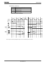
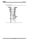
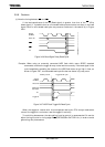
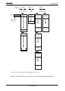
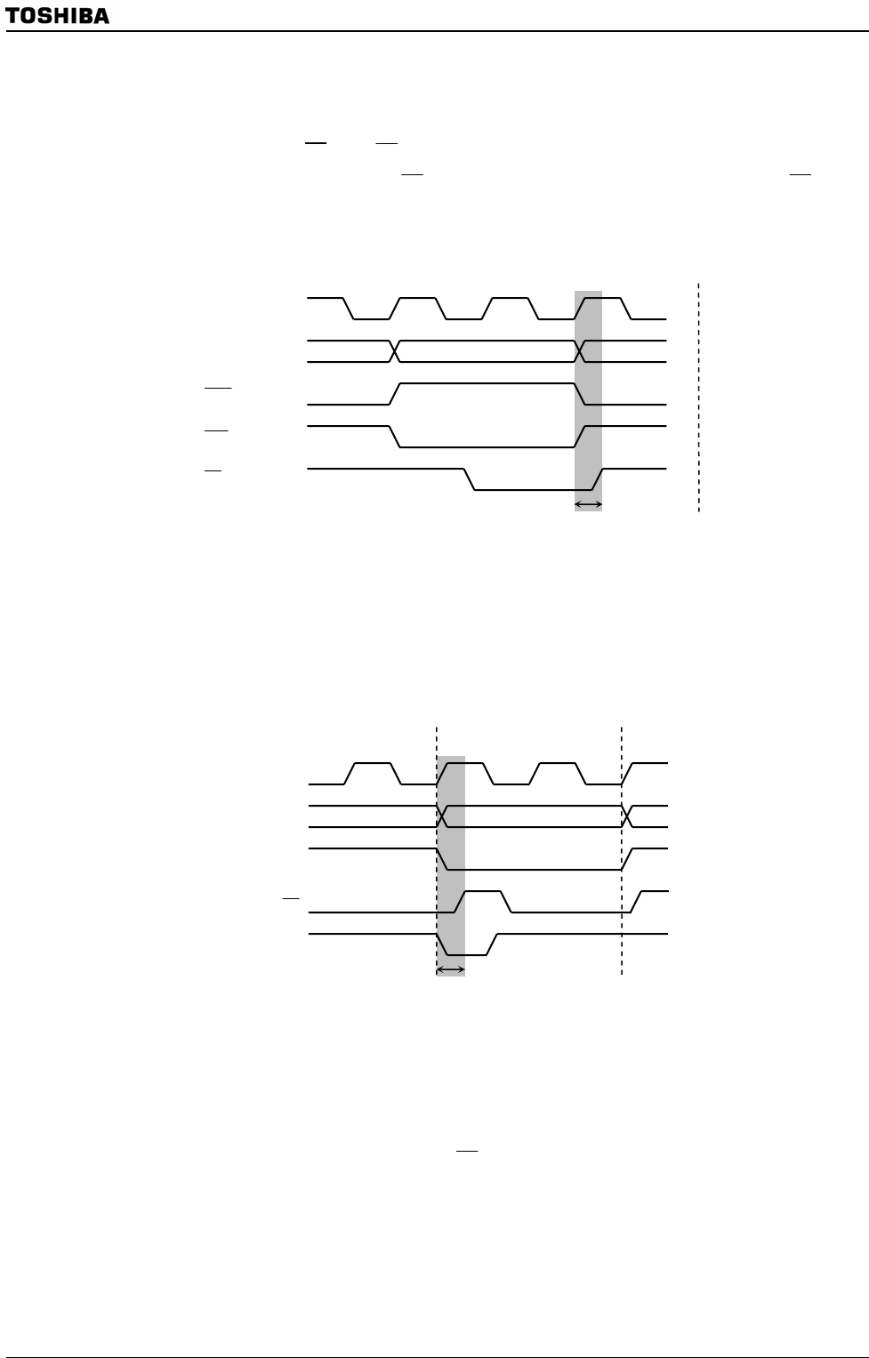
(1) Note the timing between
CS
and
RD
If the load capacitance of the
RD
(Read signal) is greater than that of the
CS
(Chip
select signal), it is possible that an unintended read cycle occurs due to a delay in the read
signal. Such an unintended read cycle may cause a trouble as in the case of (a) in
Figure
3.8.6.
Figure 3.8.6 Read Signal Delay Read Cycle
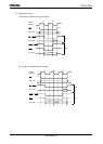
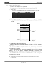
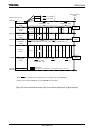
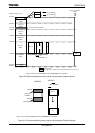
Example: When using an externally connected NOR flash which users JEDEC standard
commands, note that the toggle bit may not be read out correctly. If the read signal in the
cycle immediately preceding the access to the NOR flash does not go high in time, as
shown in
Figure 3.8.7, an unintended read cycle like the one shown in (b) may occur.
Figure 3.8.7 NOR Flash Toggle Bit Read Cycle
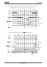
When the toggle bit reverse with this unexpected read cycle, CPU always reads same
value of the toggle bit, and cannot read the toggle bit correctly.
To avoid this phenomenon, the data polling function control is recommended. Or use the
adjust timing function for rising edge of
RD
(RDTMGCRn<BnTCRH1:0>) in order to avoid
generating this phenomenon.
RD
A
23 to A0
SDCLK
(60 MHz)
CSm
CSn
(a)
A23 to A0
SDCLK
(60 MHz)
NOR flash
chip select
RD
(b)
Toggle bit
Memory access
Toggle bit RD cycle