


TMP92CZ26A
92CZ26A-9
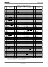
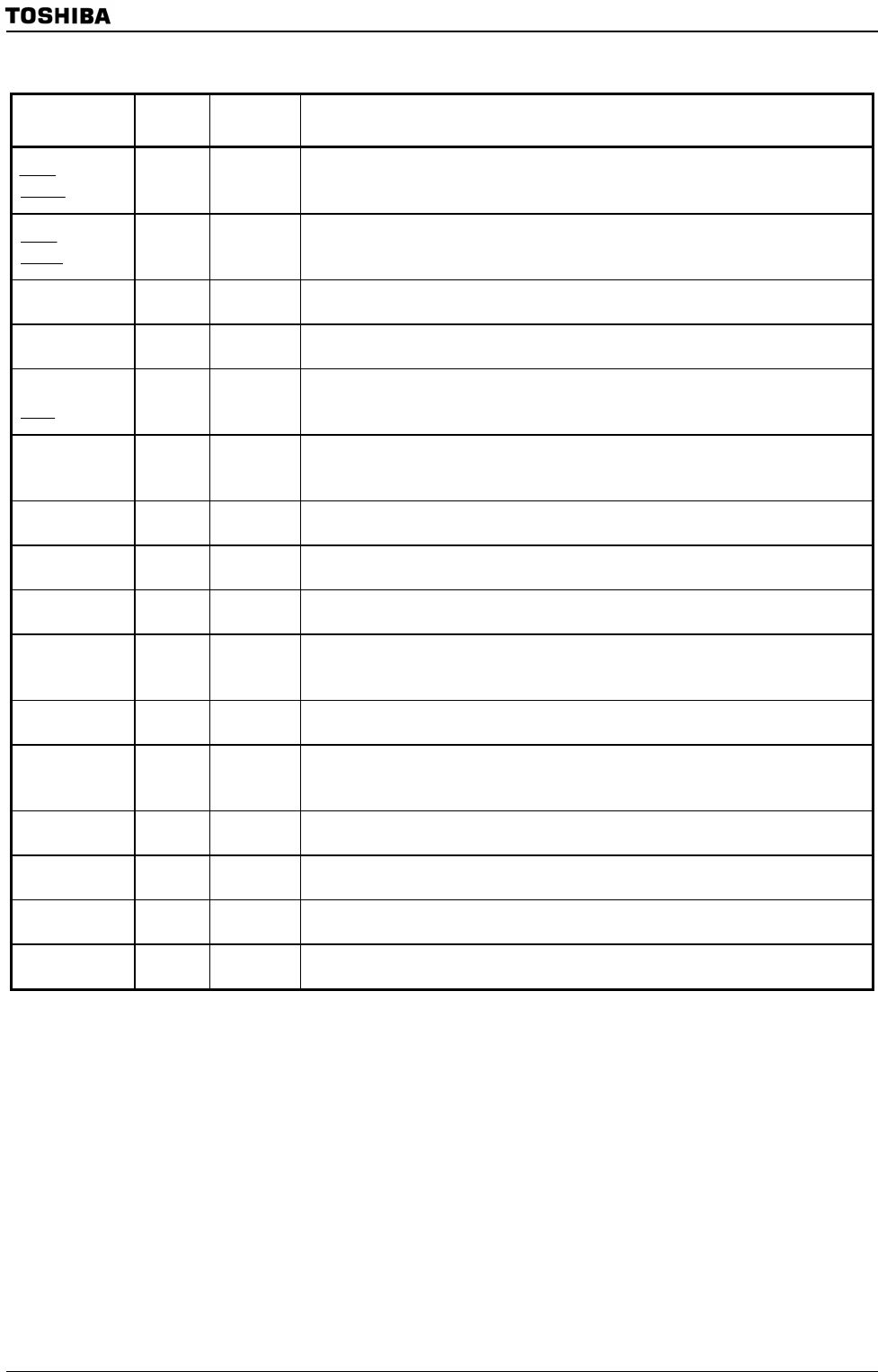
Table 2.2.1 Pin names and functions (2/6)
Pin name
Number
of Pins
I/O Functions
P86
CSZD
CE0ND
1
Output
Output
Output
Port 86 : Output port.
Expanded address ZD : Outputs “Low” when address is within specified address area.
Chip select of NAND Flash 0: Outputs “Low” when NAND Flash 0 is enable.
P87
CSXB
CE1ND
1
Output
Output
Output
Port 87 : Output port.
Expanded address XB : Outputs “Low” when address is within specified address area.
Chip select of NAND Flash 1: Outputs “Low” when NAND Flash 1 is enable.
P90
TXD0
1
I/O
Output
Port 90: I/O port.
Transmit data of serial 0: programmable open drain output.
P91
RXD0
1
I/O
Input
Port 91: I/O port. (Schmitt input)
Receive data of serial 0.
P92
SCLK0
0CTS
1
I/O
I/O
Input
Port 92: I/O port. (Schmitt input)
Clock I/O of serial 0
Enable to send data of serial 0 (Clear to send).
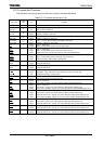
P96
INT4
PX
1 Input
Input
Output
Port 96: Input port. (schmitt input, with pull-up resistor)
Interrupt request pin 4 : Interrupt request pin with programmable rising/falling edge.
X-Plus : Pin connected to X+ pin for Touch Screen I/F.
P97
PY
1 Input
Output
Port 97: Input port. (schmitt input)
Y-Plus : Pin connected to Y+ pin for Touch Screen I/F.
PA0 to PA7
KI0 to KI7
8
Input
Input
Port A0 to A7: Input port.
Key input 0 to 7: For key on wake-up 0 to 7. (Schmitt input, with pull-up resistor)
PC0
INT0
1
I/O
Input
Port C0: I/O port. (Schmitt input)
Interrupt request pin 0 : Interrupt request pin with programmable rising/falling edge.
PC1
INT1
TA0IN
1
I/O
Input
Input
Port C1: I/O port. (Schmitt input)
Interrupt request pin 1 : Interrupt request pin with programmable rising/falling edge.
Timer A0 input: Input pin of 8 bit timer 0.
PC2
INT2
1
I/O
Input
Port C2: I/O port. (Schmitt input)
Interrupt request pin 2 : Interrupt request pin with programmable rising/falling edge.
PC3
INT3
TA2IN
1
I/O
Input
Input
Port C3: I/O port. (Schmitt input)
Interrupt request pin 3 : Interrupt request pin with programmable rising/falling edge.
Timer A2 input: Input pin of 8 bit timer 2.
PC4
EA26
1
I/O
Output
Port C4: I/O port.
Expanded address 26.
PC5
EA27
1
I/O
Output
Port C5: I/O port.
Expanded address 27.
PC6
EA28
1
I/O
Output
Port C6: I/O port.
Expanded address 28.
PC7
KO8
1
I/O
Output
Port C7: I/O port.
Key output 8: Key scan strobe pin (programmable open drain output).