


TMP92CZ26A
92CZ26A-292
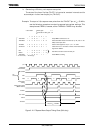
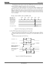
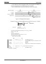
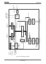
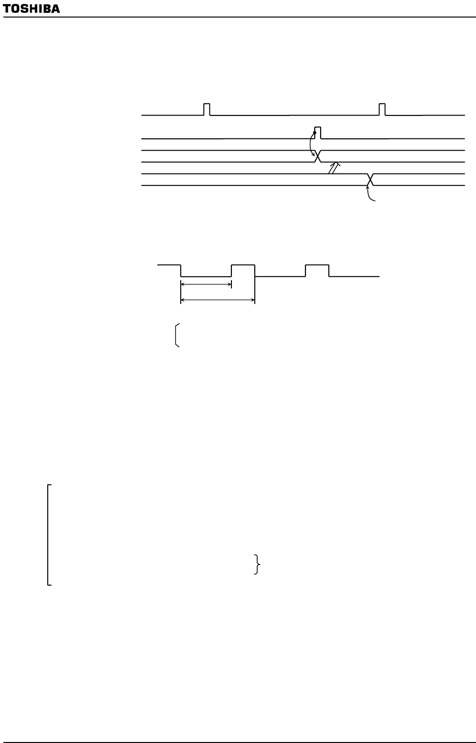
In this mode the value of the register buffer will be shifted into TA0REG if 2
n
overflow is detected when the TA0REG double buffer is enabled.
Use of the double buffer facilitates the handling of low duty ratio waves.
Figure 3.12.25 Register Buffer Operation
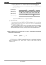
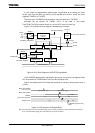
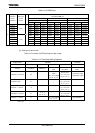
Example: To output the following PWM waves on the TA1OUT pin (at f
C
= 50 MHz).
To achieve a 20.48μs PWM cycle by setting φT1 to 0.16 μs (at f
C
= 50 MHz):
20.48 μs ÷ 0.16 μs = 128
2
n
= 128
Therefore n should be set to 7.
Since the low level period is 16.0 μs when φT1 = 0.16 μs,
set the following value for TAREG:
16.0 μs ÷ 0.16 μs = 100 = 64H
* Clock state Clcok gear : 1/1
Prescaler of clock gear : 1/2
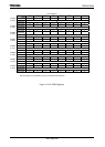
MSB LSB
7 6 5 4 3210
TA01RUN
←
−
X X X
− − −
0 Stop TMRA0 and clear it to 0
TA01MOD
←
1 1 1 0 X X 0 1 Select 8-bit PWM mode (cycle: 2
7
) and select φT1 as the
input clock.
TA0REG
←
0 1 1 0 0100 Write 64H.
TA1FFCR
←
X X X X 101X Clear TA1FF to 0, enable the inversion and double buffer.
PM
←
−
X X X X
−
00
PMFC
←
−
X X X X
−
1X
Set PM1 as the TA1OUT pin.
TA01RUN
←
1 X X X
−
1
−
1 Start TMRA0 counting.
X: Don't care, −: No change
Q
2
Q
1
Match with TA0REG
Q
3
Q
2
Up counter
=
Q
1
Up counter = Q
2
Shift into TA0REG
TA0REG (Register buffer)
write
TA0REG
(Value to be compared)
Re
g
ister buffe
r
2
n
overflow
16.0
μ
s
20.48
μ
s