TMP92CZ26A
92CZ26A-565
3.20.2 Touch Screen Interface (TSI) Control Register
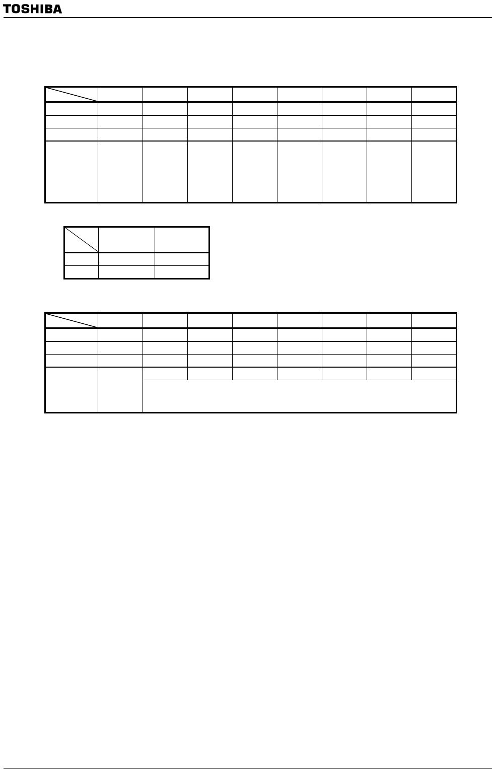
TSI control register
7 6 5 4 3 2 1 0
bit Symbol TSI7 INGE PTST TWIEN PYEN PXEN MYEN MXEN
Read/Write R/W R/W R R/W R/W R/W R/W R/W
After reset 0 0 0 0 0 0 0 0
Function
0: Disable
1: Enable
Input gate
control of
Port 96,97
0: Enable
1: Disable
Detection
condition
0: no
touch
1: touch
INT4
interrupt
control
0: Disable
1: Enable
SPY
0 : OFF
1 : ON
SPX
0 : OFF
1 : ON
SMY
0 : OFF
1 : ON
SMX
0 : OFF
1 : ON
De-bounce time setting register
7 6 5 4 3 2 1 0
bit Symbol DBC7 DB1024 DB256 DB64 DB8 DB4 DB2 DB1
Read/Write R/W R/W R/W R/W R/W R/W R/W R/W
After reset 0 0 0 0 0 0 0 0
1024 256 64 8 4 2 1
Function
0: Disable
1: Enable
De-bounce time is set by “(N*64-16) / f
SYS”-formula.
“N” is sum of number which is set to “1” in bit6 to bit 0. Note3:
Note1: Since an internal clock is used for de-bounce circuit, when IDLE1, STOP mode or PCM condition, the de-bounce
circuit don’t operate and also interrupt which through this circuit is not generated. When IDLE1, STOP mode or PCM
condition, set this circuit to disable (Write “0” to TSICR1<DBC7>) before entering HALT state.If de-bounce time is set
to “0”, signal is received after counting the 6-system clock (f
SYS
) from the condition that this circuit is set to disable.
Note2: During converting the analog input-data by using AD converter, the current flow to the normal C-MOS input-gate.
Therefore, provide its current by setting TSICR0<INGE>.If the middle voltage is inputted, cut the input-signal to
C-MOS logic (P96,P97) by settig this bit.
Note3: TSICR0<PTST> is that confirming initial pen-touch. When the input-signal to C-MOS logic is blocked by
TSICR0<INGE>, this bit is always “1”. Please be careful.
Ex:
TSICR1=95H →N = 64 + 4 + 1 = 69
TSICR0
(01F0H)
<PXEN>
<TSI7>
0 1
0
OFF OFF
1
ON OFF
PXD (internal pull-down resistor) ON/OFF setting
TSICR1
(01F1H)


