


TMP92CZ26A
92CZ26A-534
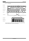
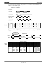
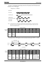
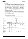
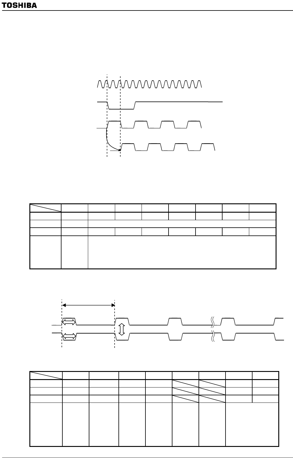
As shown in the diagram below, delay time of 0 to 127 pulses of the LCP0 clock can be
inserted in the LLOAD signal.
Delay time = <LDD6:0>
Note: The delay time for the LLOAD signal is controlled based on LCDLDDLY<PDT>=1. Therefore, even if the
delay time is set to”0” with LCDLDDLY<PDT>=0, the LLOAD signal is output with a delay of one LCP0
clock. Be careful about this point.
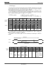
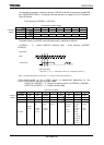
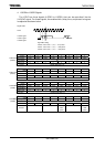
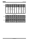
LCDLDDLY Register
7 6 5 4 3 2 1 0
bit Symbol PDT LDD6 LDD5 LDD4 LDD3 LDD2 LDD1 LDD0
Read/Write R/W W
After reset 0 0 0 0 0 0 0 0
Function
Data output
timing
0: Sync with
LLOAD
1: 1 clock later
than LLOAD
LLOAD delay (bits 6-0)
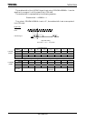
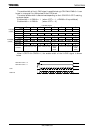
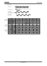
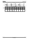
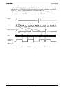
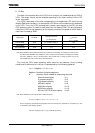
The phase of the LLOAD signal can be inverted by the setting of LCDCTL1 <LLDP>.
LCD Control 1 Register
7 6 5 4 3 2 1 0
bit Symbol LCP0P LHSP LVSP LLDP LVSW1 LVSW0
Read/Write R/W R/W R/W R/W R/W R/W
After reset 1 0 1 0 0 0
Function
LCP0
phase
0: Rising
1: Falling
LHSYNC
phase
0: Rising
1: Falling
LVSYNC
phase
0: Rising
1: Falling
LLOAD
phase
0: Rising
1: Falling
LVSYNC
enable time control
00 : 1 clock of LHSYNC
01 : 2 clocks of LHSYNC
10 : 3 clocks of LHSYNC
11 : Reserved
LCP0 signal
Signal Name
LLVSYNC signal
LHSYNC signal
(Internal reference signal)
LLOAD signal
Delay control
(Phase control)
(Enable width control)
LLDP=0
LLDP=1
LLOAD period
LLOAD signal
LCDLDDLY
(0290H)
LCDCTL1
(
0286H
)