


TMP92CZ26A
92CZ26A-500
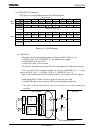
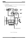
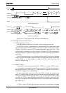
3.18.3 Description of Operation
(1) Settings the transfer clock generator and Word Select signal
In the I
2
S unit, the clock frequencies for the I2SnCKO and I2SnWS signals are
generated using the system clock (f
SYS
) as a source clock. The system clock is divided
by a prescaler and a dedicated clock generator to set the transfer clock and sampling
frequency.
The counters are started by setting I2SnCTL<CNTEn> to “1” and are stopped and
cleared by setting <CNTEn> to “0”.
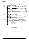
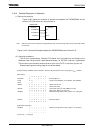
A) Clock generator
8-bit counter
This is an 8-bit counter that generates the I2SnCKO signal by dividing the clock
selected by I2SnCTL<CLKSn>.
6-bit counter
This is a 6-bit counter that generates the I2SnWS signal by dividing the
I2SnCKO signal.
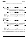
B) Word Select
Word Select signal (I2SnWS)
The I2SnWS signal is used to distinguish the position of valid data and whether
left data or right data is being transmitted in the I
2
S format. This signal is clocked
out in synchronization with the data transfer clock. In only channel 0, this signal
can be used as an AD conversion trigger signal for the ADC. How valid data is to
be output in relation to the WS signal can be specified as I
2
S format, left-justified,
or right-justified. In only channel 0, an interrupt request can be output to the ADC
on the rising edge of the WS signal. (This is controlled by the ADC’s control
register.)
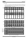
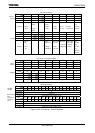
(2) Data format
This circuit support I2S format, left justify and right justify format by setting
I2SnCTL<DTFMTn1:n0> register. And support stereo and monaural both, controlled
by I2SnCTL<FSELn> register.