TMP92CZ26A
92CZ26A-194
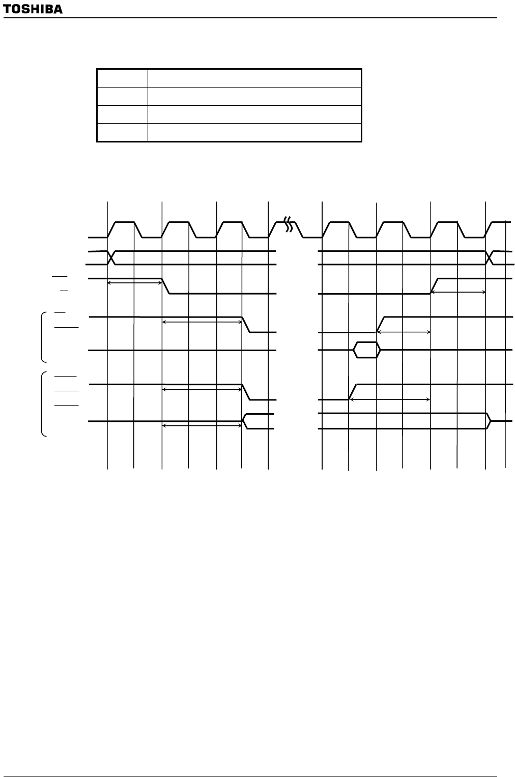
RDTMGCR0/1<BnTCRS1:0>
00 TCRS = 0.5 × f
SYS
(Default)
01 TCRS = 1.5 × f
SYS
10 TCRS = 2.5 × f
SYS
11 TCRS = 3.5 × f
SYS
TCRS:The delay from (CSn) to (RD,SRxxB).
Note: TW cycle is inserted by setting BnCSL register. If it is set to 0-Wait, TW cycle is not inserted.
A23 to 0
CSn
R/
W
T1
T2
SDCLK
(80MHz)
RD
SRxxB
Input
D15 to 0
Read
cycle
T3
Tn
TAC
TCRS
TCRH
Tn
-
1
WRxx
SRWR
SRxxB
D15 to 0
TCWS
TCWH
TAC
Output
Tn
-
2
Write
cycle
Output
TCWS
TW


