


TMP92CZ26A
92CZ26A-142
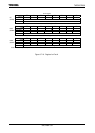
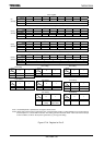
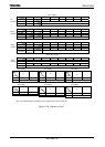
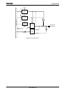
Port F register
7 6 5 4 3 2 1 0
bit Symbol PF7 PF5 PF4 PF3 PF2 PF1 PF0
Read/Write R/W R/W
After reset 1 Data from external port (Output latch register is set to “1”)
Port F control register
7 6 5 4 3 2 1 0
bit Symbol PF5C PF4C PF3C PF2C PF1C PF0C
Read/Write W
After reset 0 0 0 0 0 0
Function Refer to following table
Port F function register
7 6 5 4 3 2 1 0
bit Symbol PF7F PF5F PF4F PF3F PF2F PF1F PF0F
Read/Write W W
After reset 1 0 0 0 0 0 0
Function
0: Port
1: SDCLK
Refer to following table
Port F drive register
7 6 5 4 3 2 1 0
bit Symbol PF7D PF6D PF5D PF4D PF3D PF2D PF1D PF0D
Read/Write R/W
After reset 1 1 1 1 1 1 1 1
Function Input/Output buffer drive register for standby mode
Note 1: Read-Modify-Write is prohibited for the registers PFCR, PFFC and PFFC2.
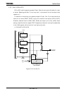
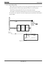
Figure 3.7.28 Register for Port F
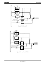
PFFC
(003FH)
PF
(003CH)
PFCR
(003EH)
PFDR
(008FH)
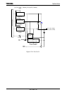
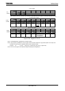
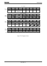
<PF0C>
<PF0F>
0 1
0 Input port Output port
1 I2S0CKOoutput
PF0 setting
<PF1C>
<PF1F>
0 1
0 Input port Output port
1 I2S0DO output
PF1 setting
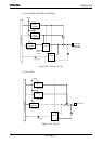
<PF2C>
<PF2F>
0 1
0 Input port Output port
1 I2S0WS output
PF2 setting
<PF3C>
<PF3F>
0 1
0 Input port Output port
1
I2S1CKOoutput
PF3 setting
<PF4C>
<PF4F>
0 1
0 Input port Output port
1 I2S1DO output
PF4 setting
<PF5C>
<PF5F>
0 1
0 Input port Output port
1 I2S1WS output
PF5 setting