TMP92CZ26A
92CZ26A-158
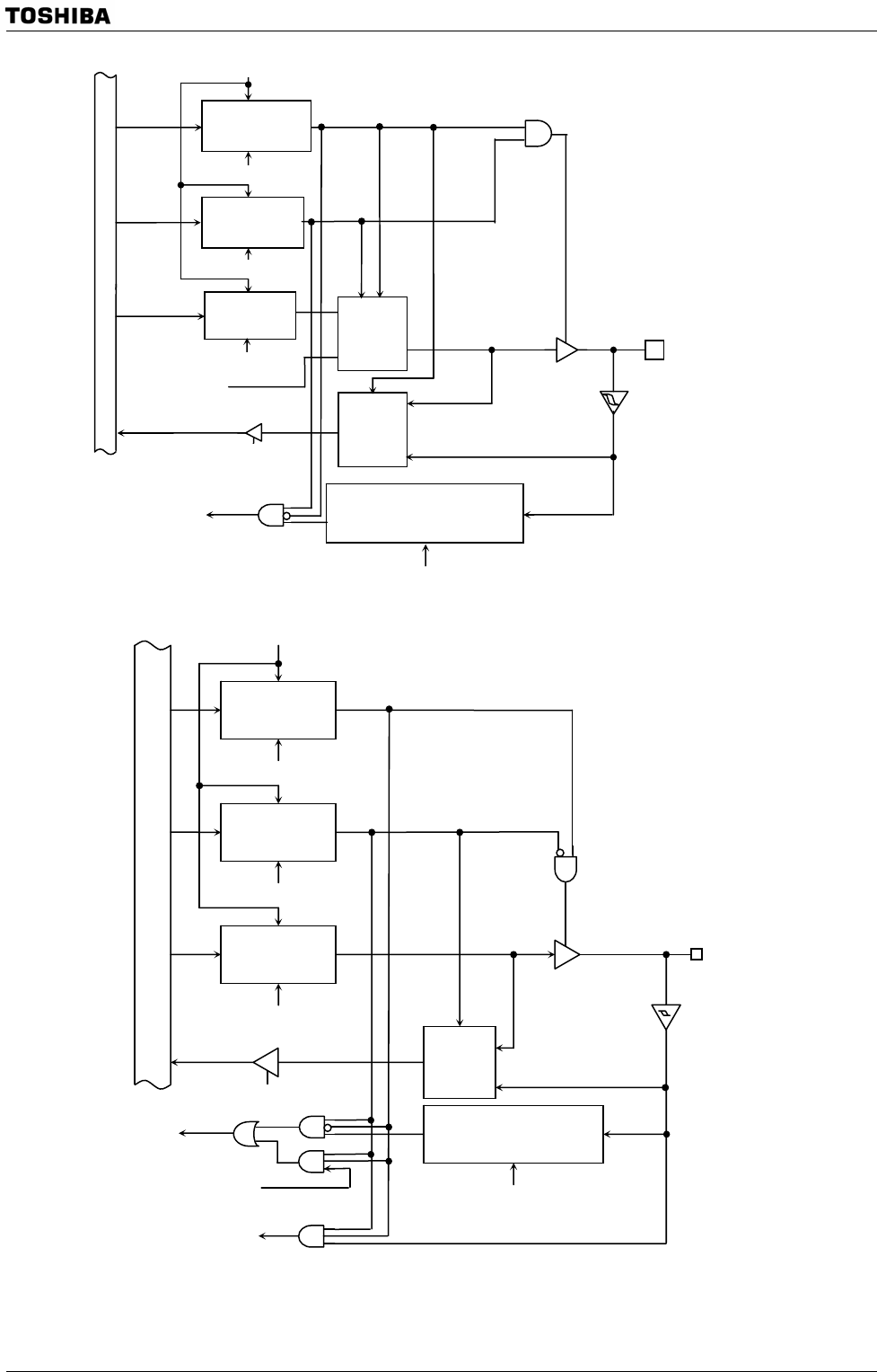
Figure 3.7.45 Port P3
Figure 3.7.46 Port P4,P5
PP4 (INT6,TB0IN0)
PP5 (INT7, TB1IN0)
Internal data bus
Direction control
(on bit basis)
Reset
PPCR write
PP write
PP read
Function control
(on bit basis)
PPFC write
R
Output latch
S
B
Selector
A
Level/edge selection
and
Rising/Falling selection
IIMC<I1LE, I1EDGE>
<I3LE, I3EDGE>
INT6
INT7
TB0IN0
TB1IN0
(from TMRB0) INT6
(from TMRB1) INT7
Selector
A
B
S
PP3 (INT5, TA7OUT)
PP read
Direction control
(on bit basis)
PPCR write
Function
control
(on bit basis)
R
Output latch
PP write
Reset
PPFC write
Level/edge selection
and
Rising/Falling selection
INT5
IIMC<I5LE, I5EDGE>
Selector
B
A
S
Internal data bus
TA7OUT


