


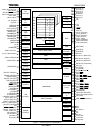
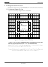

TMP92CZ26A
92CZ26A-13
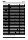
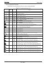
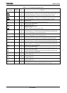
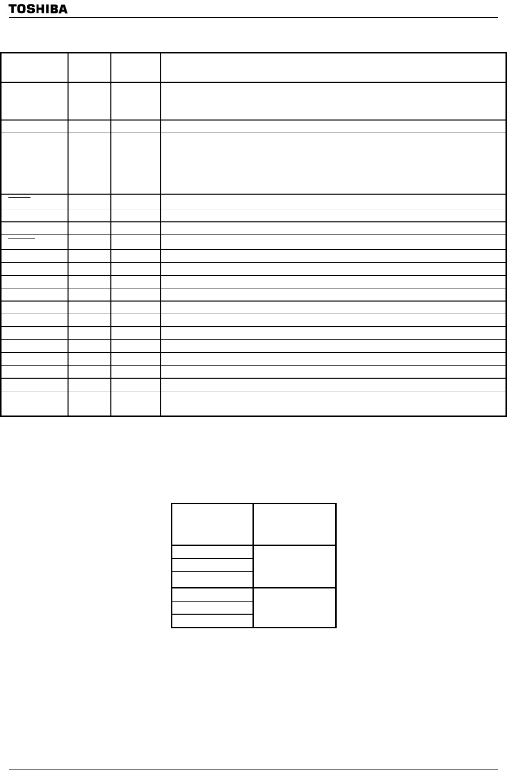
Table 2.2.1 Pin names and functions (6/6)
Pin name
Number of
Pins
I/O Functions
D+, D- 2 I/O
Data pin connected to USB.
In case USB is not used, connect both pins to pull-up(DVCC3A) or pull-down resistor for protect
current flows it.
CLKOUT 1 Output Internal clock output pin.
AM1,AM0 2 Input
Operation mode;
Fix to AM1=”0”,AM0=”1” for 16 bit external bus starting.
Fix to AM1=”1”,AM0=”0” is prohibit to set.
Fix to AM1=”1”,AM0=”1” for BOOT (32 bit internal Mask ROM) starting.
Fix to AM1=”0”,AM0=”0” is prohibited to set.
DBGE
1 Input Input pin in debug mode. (This pin is set to “Debug mode” by input “0”.)
X1/X2 2 I/O High-frequency oscillator circuit connection pin.
XT1/XT2 2 I/O Low-frequency oscillator circuit connection pin.
RESET
1 Input Reset : Initialize TMP92CZ26A (schmitt input , with pull-up resistor)
VREFH 1 Input Pin for reference voltage input to A/D converter(H).
VREFL 1 Input Pin for reference voltage input to A/D converter(L).
AVCC 1
−
Power supply pin for A/D converter.
AVSS 1
−
GND pin for AD converter (0V).
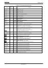
DVCC3A 12
−
Power supply pin for peripheral I/O-A (Connect all DVCC3A pins to power supply pin.)
DVCC3B 1
−
Power supply pin for peripheral I/O-B (Connect all DVCC3B pins to power supply pin.)
DVCC1A 5
−
Power supply pin for internal logic-A. (Connect all DVCC1A pins to power supply pin.)
DVCC1B 1
−
Power supply pin for internal logic-B. (Keep the voltage DVCC1A level.)
DVSSCOM 12
−
GND pin (0V). (Connect all DVSS pins to GND(0V).)
DVCC1C 1
−
Power supply pin for High speed oscillator. (Keep the voltage DVCC1A level.)
DVSS1C 1
−
GND pin (0V). (Connect to GND(0V).)
Dummy4-1 4
−
Dummy1 and Dummy2, Dummy3 and Dummy4 are shorted in package. (These pins are not
connected with internal LSI chip.)
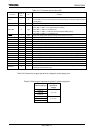
Table 2.2.2 shows the range of operational voltage for power supply pins.
Table 2.2.2 the range of operational voltage for power supply pins
Power supply pin
Range of
operational
voltage
DVCC1A
DVCC1B
DVCC1C
1.4V~1.6V
DVCC3A
DVCC3B
AVCC
3.0V~3.6V