


TMP92CZ26A
92CZ26A-15
3.1.2 Reset Operation
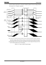
When resetting the TMP92CZ26A microcontroller, ensure that the power supply voltage
is within the operating voltage range, and that the internal high-frequency oscillator has
stabilized. Then hold the
RESET input Low for at least 20 system clocks (32µs at
X1=10MHz).
At reset, since the clock doublers (PLL0) is bypassed and clock-gear is set to 1/16, system
clock operates at 625 kHz(X1=10MHz).
When the Reset has been accepted, the CPU performs the following. CPU internal
registers do not change when the Reset is released.
• Sets the Stack Pointer (XSP) to 00000000H.
• Sets bits <IFF2:0> of the Status Register (SR) to “111” (thereby setting the Interrupt
Level Mask Register to level 7).
• Clears bits <RFP1:0> of the Status Register to 00 (thereby selecting Register Bank 0).
When the Reset is released, the CPU starts executing instructions according to the
Program Counter settings.
• Sets the Program Counter (PC) as follows in accordance with the Reset Vector stored
at address FFFF00H~FFFF02H:
PC<7:0> ← data in location FFFF00H
PC<15:8> ← data in location FFFF01H
PC<23:16> ← data in location FFFF02H
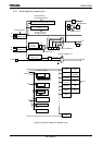
When the Reset is accepted, the CPU sets internal I/O, ports and other pins as follows.
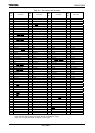
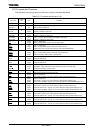
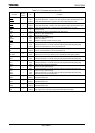
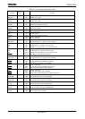
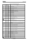
• Initializes the internal I/O registers as table of “Special Function Register” in Section
5.
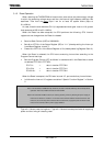
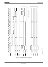
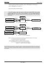
Figure 3.1.2 shows reset timing chart. Figure 3.1.2 shows the example of order of supplying
power and the timing of releasing reset.
Note1: This LSI builds in RAM internally. However, the data in internal RAM may not be held by Reset
operation. After reset, initialize the data in internal RAM.
Note2: This LSI builds in PMC function (for reducing stand-by current by blocking the power supply of
DVCC1A and DVCC1C). However, if executing reset operation without supplying DVCC1A and
DVCC1C, the current may flow to internal. When reset this LSI, supply the power of DVCC1A and
DVCC1C first and wait until the power supply stabilizes.