


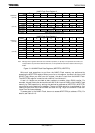
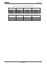

TMP92CZ26A
92CZ26A-247
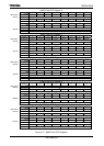
(c) <ECCE>
The <ECCE> bit is used for both Hamming and Reed-Solomon codes.
This bit is used to enable or disable the ECC generator. To reset the ECC in the ECC
generator (to set <ECCRST> to “1”), the ECC generator must be enabled (<ECCE> = “1”).
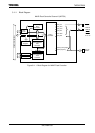
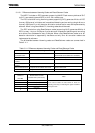
(d) <CE1:0>, <CLE>, <ALE>
The <CE1:0>, <CLE>, and <ALE> bits are used for both Hamming and Reed-Solomon
codes to control the pins of the NAND Flash memory.
(e) <WE>
The <WE> bit is used for both Hamming and Reed-Solomon codes to enable or disable
write operations.
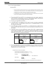
(f) <RSECGW>
The <RSECGW> bit is used only for Reed-Solomon codes. When Hamming codes are used,
this bit should be set to “0”.
Since valid data and ECC are processed differently, the NDFC needs to know whether
valid data or ECC is to be read. This control is implemented by software using this bit.
To read valid data from the NAND Flash, set <RSECGW> to “0”. To read ECC written in
the redundant area in the NAND Flash, set <RSECGW> to “1”.
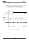
Note 1: Valid data and ECC cannot be read continuously by DMA transfer. After valid data has been read, DMA
transfer should be stopped once to change the <RSECGW> bit from “0” to “1” before ECC can be read.
Note 2: Immediately after ECC is read from the NAND Flash, the NAND Flash access operation or error bit
calculation cannot be performed for a duration of 20 system clocks (f
SYS
). It is necessary to insert 20 NOP
instructions or the like.
(g) <RSESTA>
The <RSESTA> bit is used only for Reed-Solomon codes.
The error address and error bit position are calculated using an intermediate code
generated from the ECC for written data and the ECC for read data. Setting <RSESTA> to
“1” starts this calculation.
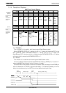
(h) <RSEDN>
The <RSEDN> bit is used only for Reed-Solomon codes. When using Hamming codes, this
bit should be set to “0”.
For a write operation, this bit should be set to “0” (encode) to generate ECC. The ECC
read from the NDECCRDn register is written to the redundant area in the NAND Flash.
For a read operation, this bit should be set to “1” (decode). In this case, valid data is read
from the NAND Flash and the ECC written in the redundant area is also read to generate
an intermediate code for calculating the error address and error bit position.