


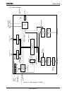
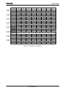
TMP92CZ26A
92CZ26A-303
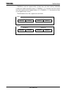
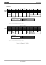
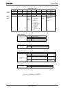
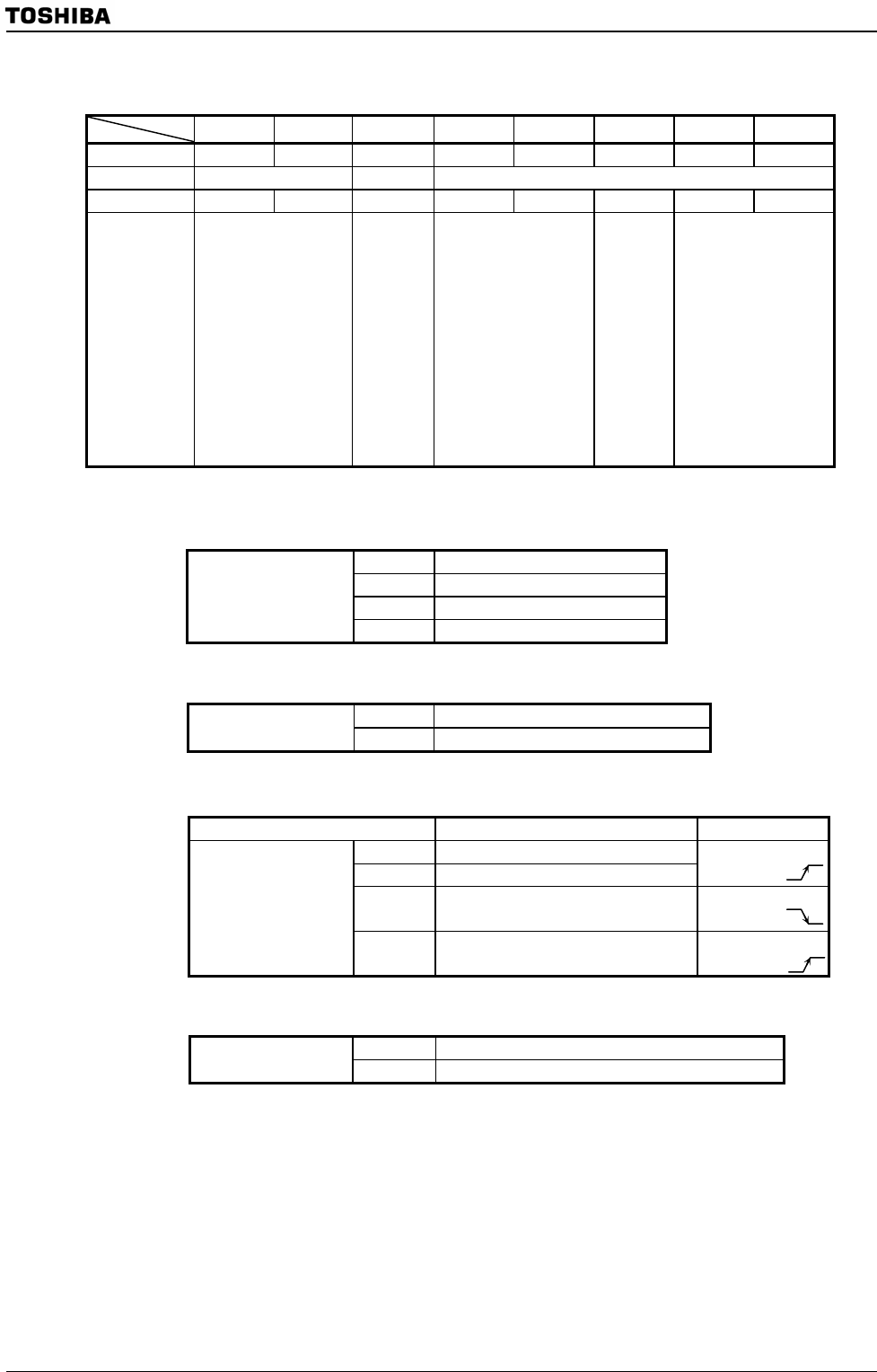
TMRB0 Mode Register
7 6 5 4 3 2 1 0
Bit symbol
− −
TB0CP0I TB0CPM1 TB0CPM0 TB0CLE TB0CLK1 TB0CLK0
Read/Write R/W
W*
R/W
After Reset 0 0 1 0 0 0 0 0
Function Always write “0”.
Software
capture control
0: Execute
1: Undefined
Capture timing
00:Disable
INT6 occurs at
rising edge
01:TB0IN0 ↑
INT6 occurs at
rising edge
10: TB0IN0 ↑ TB0IN0 ↓
INT6 occurs at
falling edge
11: TA1OUT ↑
TA1OUT ↓
INT6 occurs at rising
edge
Control
Up counter
0:Disable
1: Enable
TMRB0 source clock
00: TB0IN0 input
01: φT1
10: φT4
11: φT16
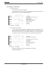
Figure 3.13.4 Register for TMRB (2)
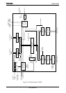
TMRB0 source clock
00 TB0IN0 pin input
01 φT1
10 φT4
<TB0CLK1:0>
11 φT16
Control clearing for up counter (UC10)
0 Disable
<TB0CLE>
1 Enable clearing by match with TB0RG1
Capture/interrupt timing
Capture control INT6 control
00 Disable
01
Capture to TB0CP0H/L at rising edge of TB0IN0
INT6 occurs at the rising
edge of TB0IN0
10
Capture to TB0CP0H/L at rising edge of TB0IN0
Capture to TB0CP1H/L at falling edge of TB0IN0
INT6 occurs at the rising
edge of TB0IN0
<TB0CPM1:0>
11
Capture to TB0CP0H/L at rising edge of TA1OUT
Capture to TB0CP1H/L at falling edge of TA1OUT
INT6 occurs at the rising
edge of TB0IN0
Software capture
0 The value of up counter is captured to TB0CP0H/L
<TB0CP0I>
1 Undefined
TB0MOD
(1182H)
Prohibit
read-
modify-
write