


TMP92CZ26A
92CZ26A-523
3.19.3.5 Refresh Rate
The period of the horizontal synchronization signal LHSYNC is defined as the
product of the value set in LCDHSP<LH15:0> and the LCP0 clock period.
The value to be set in LCDHSP<LH15:0> is obtained as follows:
TFT
Segment size + number of dummy clocks
(*)
STN
Monochrome/grayscale : (Segment size / 8) + number of dummy clocks
(*)
Color : (Segment size × 3 / 8) + number of dummy clocks
(*)
LHSYNC [s: period] = LCP0 [s: period] × (<LH15:0> + 1)
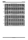
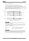
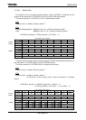
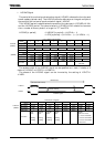
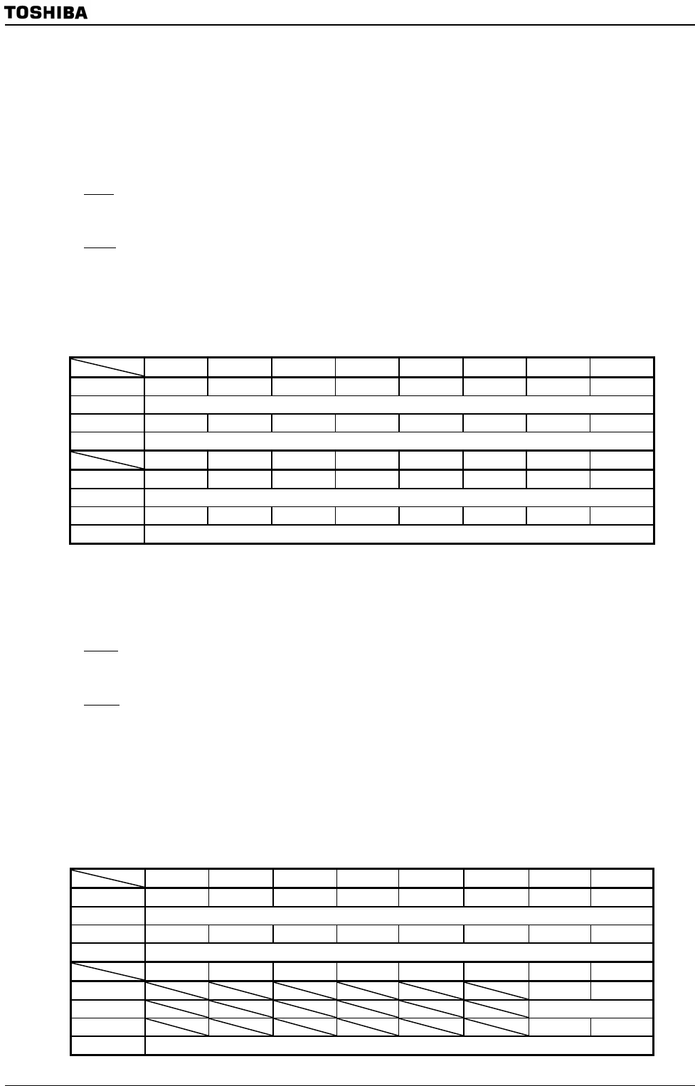
LCD LHSYNC Pulse Register
7 6 5 4 3 2 1 0
bit Symbol LH7 LH6 LH5 LH4 LH3 LH2 LH1 LH0
Read/Write W
After reset 0 0 0 0 0 0 0 0
Function LHSYNC period (bits 7–0)
7 6 5 4 3 2 1 0
bit Symbol LH15 LH14 LH13 LH12 LH11 LH10 LH9 LH8
Read/Write W
After reset 0 0 0 0 0 0 0 0
Function LHSYNC period (bits 15-8)
The period of the vertical synchronization signal LVSYNC is defined as the product of
the value set in LCDVSP<LV9:0> and the LHSYNC period.
The value to be set in LCDVSP<LV9:0> is obtained as follows:
TFT
Common size + number of dummy clocks
(*)
STN
Common size + number of dummy clocks
(*)
(A minimum of one dummy clock must be inserted in the back
porch.)
LVSYNC [s: period] = LHSYNC [s: period] × (<LV9:0> + 1)
= LCP0 [s: period] × (<LH15:0> + 1) × (<LV9:0> + 1)
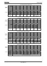
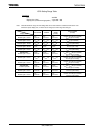
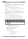
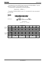
LCD V SYNC Pulse Register
7 6 5 4 3 2 1 0
bit Symbol LVP7 LVP6 LVP5 LVP4 LVP3 LVP2 LVP1 LVP0
Read/Write W
After reset 0 0 0 0 0 0 0 0
Function LVSYNC period (bits 7-0)
7 6 5 4 3 2 1 0
bit Symbol LVP9 LVP8
Read/Write W
After reset 0 0
Function LVSYNC period (bits 9-8)
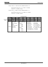
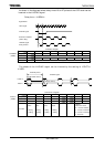
LCDHSP
(
028AH
)
(028BH)
LCDVSP
(
028CH
)
(028DH)