


TMP92CZ26A
92CZ26A-6
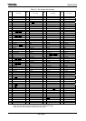
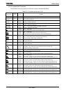
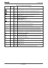
2. Pin Assignment and Pin Functions
The assignment of input/output pins for TMP92CZ26A, their names and functions are as follows;
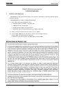
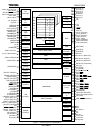
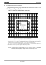
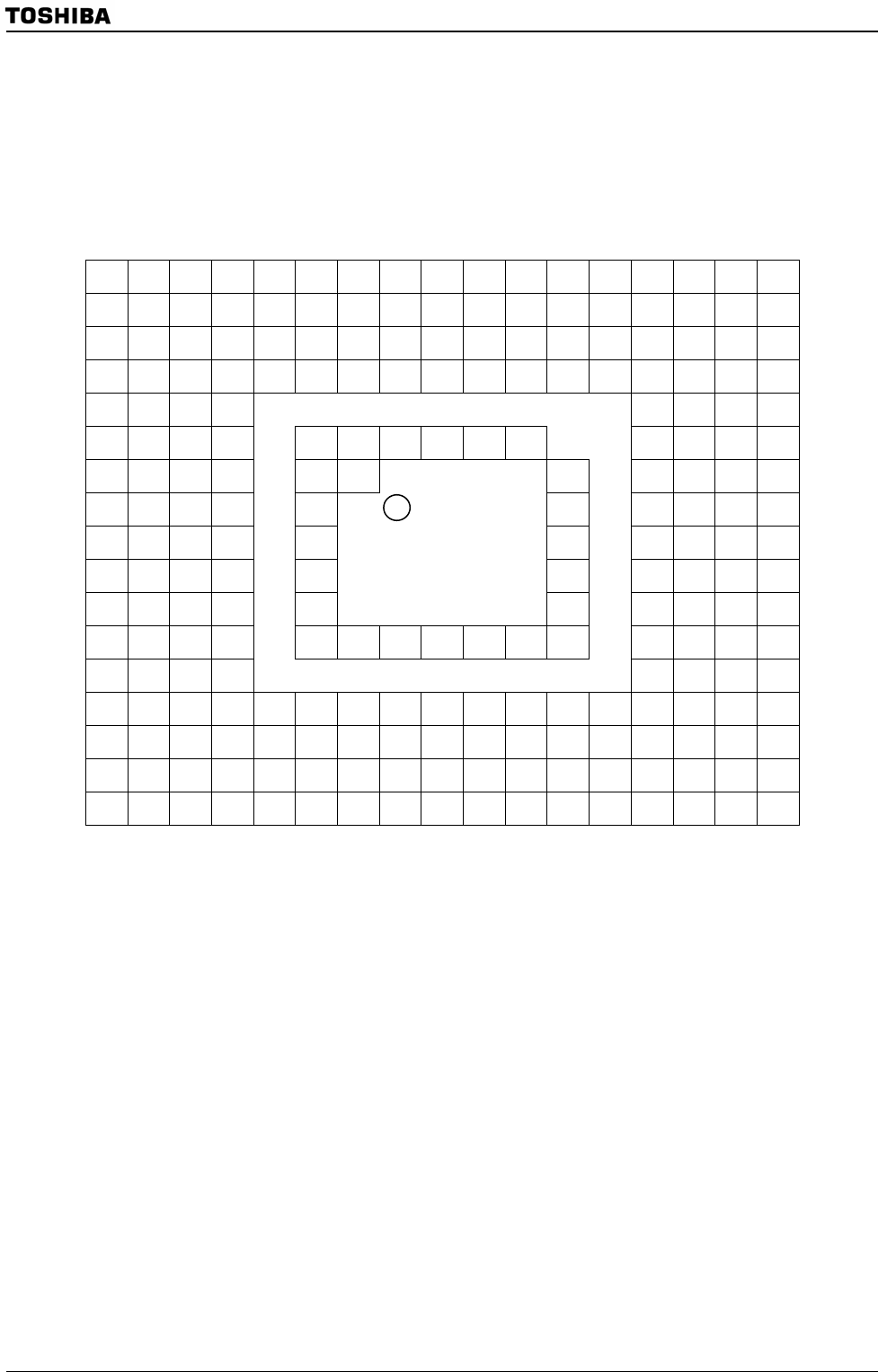
2.1 Pin Assignment Diagram (Top View)
Figure 2.1.1 shows the pin assignment of the TMP92CZ26A.
A1 A2 A3 A4 A5 A6 A7 A8 A9 A10 A11 A12 A13 A14 A15 A16 A17
B1 B2 B3 B4 B5 B6 B7 B8 B9 B10 B11 B12 B13 B14 B15 B16 B17
C1 C2 C3 C4 C5 C6 C7 C8 C9 C10 C11 C12 C13 C14 C15 C16 C17
D1 D2 D3 D5 D6 D7 D8 D9 D10 D11 D12 D13 D15 D16 D17
E1 E2 E3 E4 E14 E15 E16 E17
F1 F2 F3 F4 F6 F7 F8 F9 F10 F11 F14 F15 F16 F17
G1 G2 G3 G4 G6 G7 G12 G14 G15 G16 G17
H1 H2 H3 H4 H6 H12 H14 H15 H16 H17
J1 J2 J3 J4 J6 J12 J14 J15 J16 J17
K1 K2 K3 K4 K6 K12 K14 K15 K16 K17
L1 L2 L3 L4 L6 L12 L14 L15 L16 L17
M1 M2 M3 M4 M6 M7 M8 M9 M10 M11 M12 M14 M15 M16 M17
N1 N2 N3 N4 N14 N15 N16 N17
P1 P2 P3 P5 P6 P7 P8 P9 P10 P11 P12 P13 P15 P16 P17
R1 R2 R3 R4 R5 R6 R7 R8 R9 R10 R11 R12 R13 R14 R15 R16 R17
T1 T2 T3 T4 T5 T6 T7 T8 T9 T10 T11 T12 T13 T14 T15 T16 T17
U1 U2 U3 U4 U5 U6 U7 U8 U9 U10 U11 U12 U13 U14 U15 U16 U17
Figure 2.1.1 Pin assignment diagram (P-FBGA228)
4 balls of A1, A17, U1 and U17 (most outside 4 corner of BGA package) are Dummy Balls.
These balls are not connected with internal LSI chip, electrical characteristics.
A1 and U1, A17 and U17 are shorted in internal package. It is recommended that using to
OPEN check of mounting if mounting this LSI to Target board.
Example: If checking signal (or voltage) via A1-U1-U17-A17, short U17 and U1 on Target board
beforehand, and input signal (or voltage) from A1, and check voltage of A17.
TMP92CZ26A
P-FBGA228
TOP VIEW