


TMP92CZ26A
92CZ26A-635
2) Pins
In debug mode, a total of 9 pins (PZ0 to PZ7 in Port Z and PU7 in Port U) are used to
connect the TMP92CZ26A with an emulator via a DSU probe for communicating with the
controller. For this reason, these 9 pins cannot be debugged. Therefore, if the port control
register of each pin is changed in debug mode, the register contents are changed but the
function of each pin remains the same.
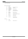
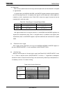
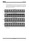
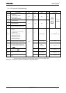
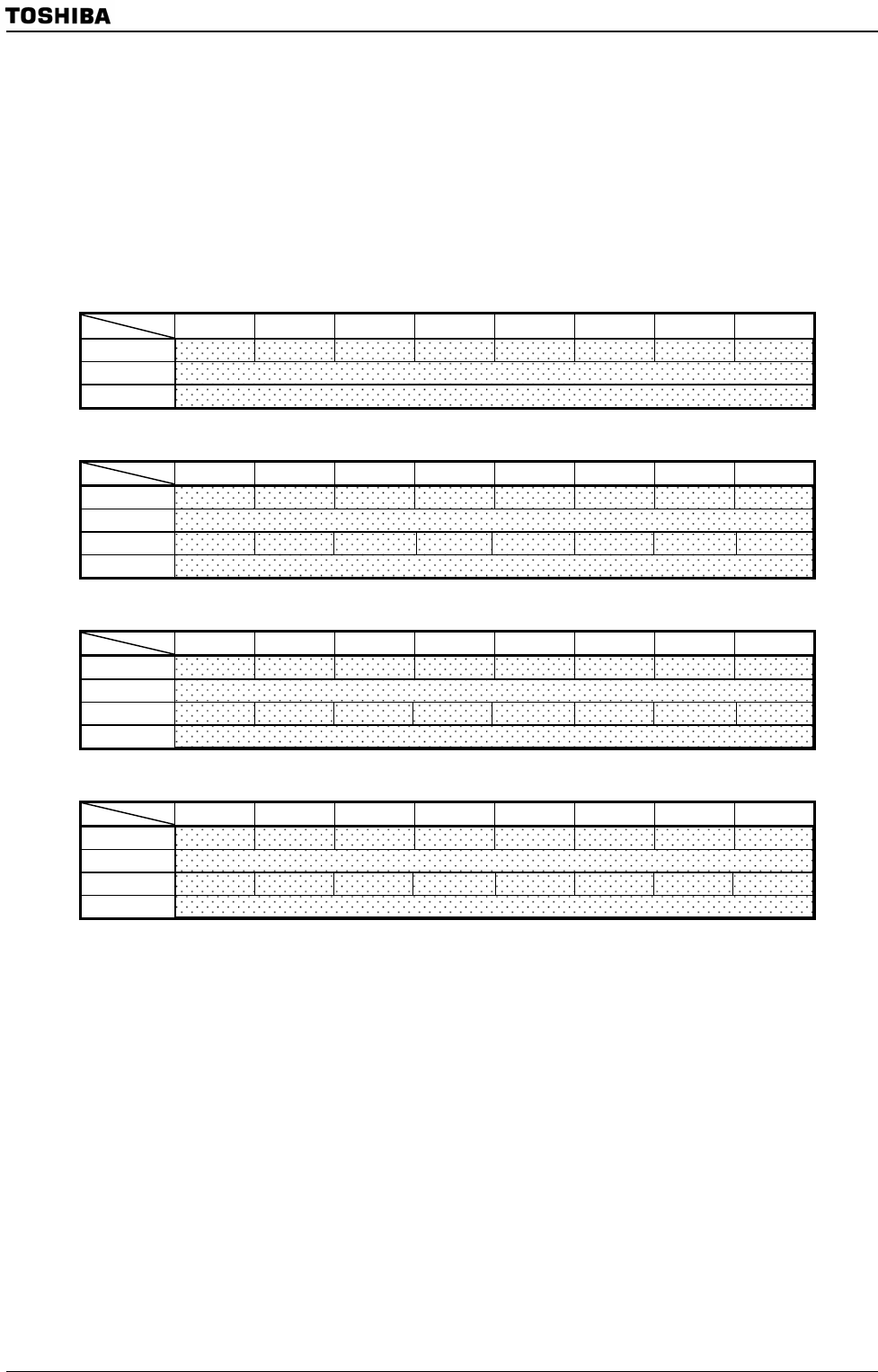
Port Z Register
7 6 5 4 3 2 1 0
bit Symbol PZ7 PZ6 PZ5 PZ4 PZ3 PZ2 PZ1 PZ0
Read/Write R/W
After reset External pin data (Output latch is reset to “0”.)
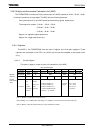
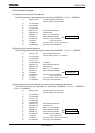
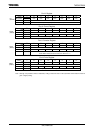
Port Z Control Register
7 6 5 4 3 2 1 0
bit Symbol PZ7C PZ6C PZ5C PZ4C PZ3C PZ2C PZ1C PZ0C
Read/Write W
After reset 0 0 0 0 0 0 0 0
Function 0: Input 1: Output
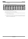
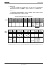
Port Z Function Register
7 6 5 4 3 2 1 0
bit Symbol PZ7F PZ6F PZ5F PZ4F PZ3F PZ2F PZ1F PZ0F
Read/Write W
After reset 0 0 0 0 0 0 0 0
Function 0: Port
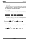
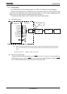
Port Z Drive Register
7 6 5 4 3 2 1 0
bit Symbol PZ7D PZ6D PZ5D PZ4D PZ3D PZ2D PZ1D PZ0D
Read/Write R/W
After reset 1 1 1 1 1 1 1 1
Function Input/output buffer drive register for standby mode
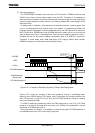
Note: Although it is possible to write to shaded bits, writing to these bits has no effect (the DSU communication function is
given a higher priority).
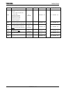
PZCR
(006AH)
PZDR
(009AH)
PZFC
(006BH)
PZ
(0068H)