


TMP92CZ26A
92CZ26A-34
3.3.6 Standby controller
(1) Halt Modes and Port Drive-register
When the HALT instruction is executed, the operating mode switches to IDLE2,
IDLE1 or STOP Mode, depending on the contents of the SYSCR2<HALTM1 to 0>
register and each pin-status is set according to PxDR-register.
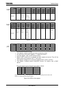
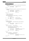
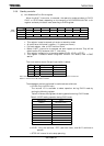
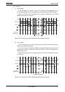
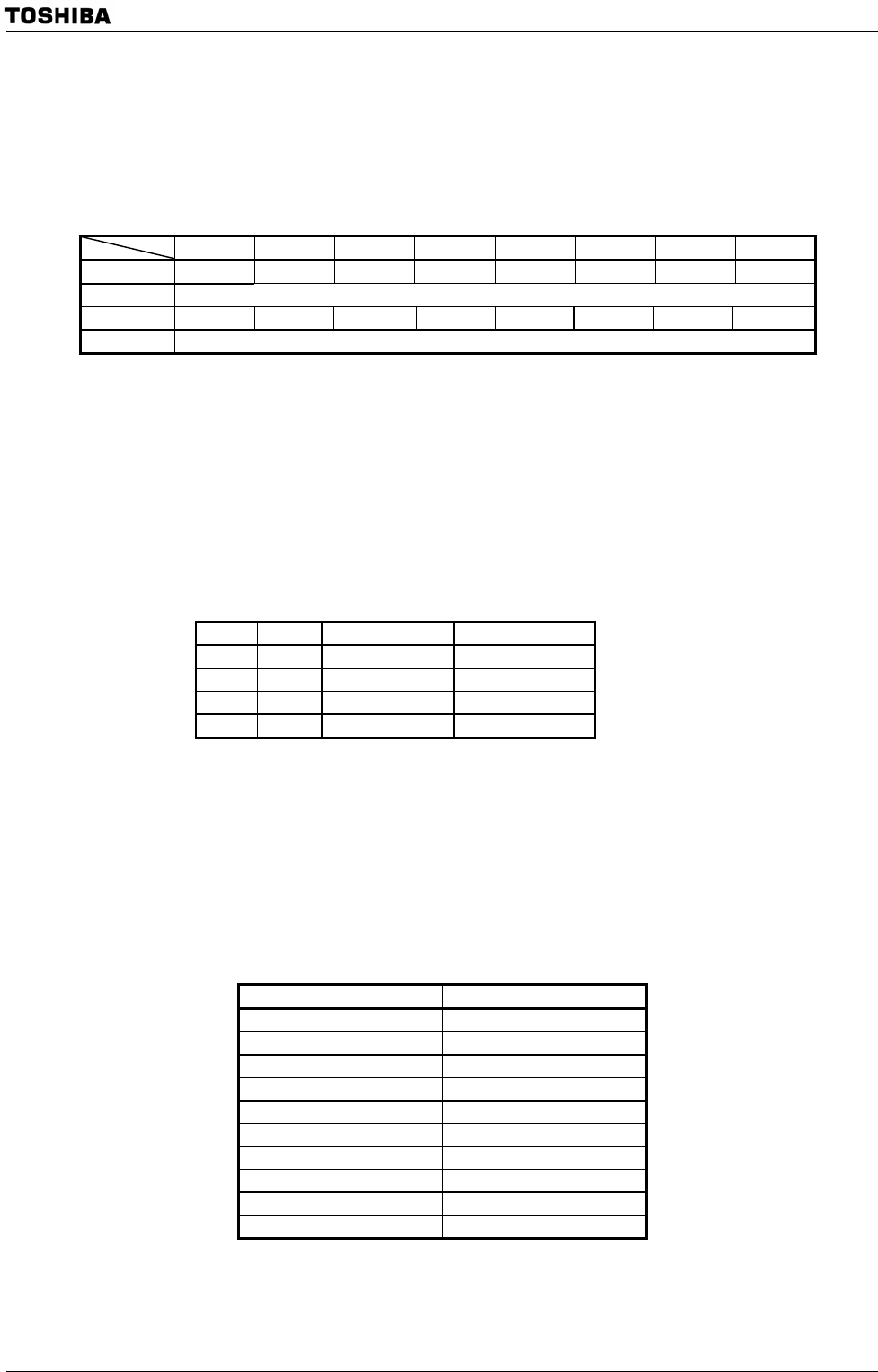
7 6 5 4 3 2 1 0
bit symbol Px7D Px6D Px5D Px4D Px3D Px2D Px1D Px0D
Read/Write R/W
After reset 1 1 1 1 1 1 1 1
Function Output/Input buffer drive-register for standby-mode
(Purpose and method of using)
• This register is used to set each pin-status at stand-by mode.
• All ports have this format’s register. (“x” means port-name.)
• For each register, refer to 3.5 Function of Ports.
• Before “HALT” instruction is executed, set each register pin-status. They will be
effective after CPU executes “HALT” instruction.
• This register is effective in all stand-by modes (IDLE2, IDLE1 or STOP).
• This register is effective when using PMC function. For details, refer to PMC
section.
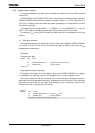
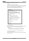
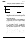
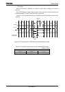
The truth table to control Output/Input-buffer is below.
OE PxnD Output buffer Input buffer
0 0 OFF OFF
0 1 OFF ON
1 0 OFF OFF
1 1 ON OFF
Note1: OE means an output enable signal before stand-by mode.Basically, PxCR is used as OE.
Note2: “n” in PxnD means bit-number of PORTx.
The subsequent actions performed in each mode are as follows:
a. IDLE2: Only the CPU halts.
The internal I/O is available to select operation during IDLE2 mode by
setting the following register.
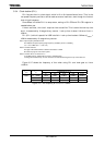
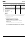
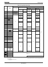
Table 3.3.2 shows the registers of setting operation during IDLE2 mode.
Table 3.3.2 SFR setting operation during IDLE2 mode
Internal I/O SFR
TMRA01 TA01RUN<I2TA01>
TMRA23 TA23RUN<I2TA23>
TMRA45 TA45RUN<I2TA45>
TMRA67 TA67RUN<I2TA67>
TMRB0 TB0RUN<I2TB0>
TMRB1 TB1RUN<I2TB1>
SIO0 SC0MOD1<I2S0>
SBI SBIBR0<I2SBI>
A/D converter ADMOD1<I2AD>
WDT WDMOD<I2WDT>
b. IDLE1: Only the oscillator, RTC (real-time clock), and MLD continue to
operate.
c. STOP: All internal circuits stop operating.
PxDR
(xxxxH)