


TMP92CZ26A
92CZ26A-208
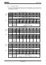
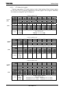
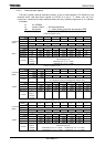
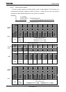
3.9.2 Control register
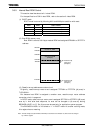
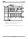
There are 24-registers for MMU. They are prepared for 8-purpose using (as Program,
read-data, write-data and LCDC-display-data, source-data for odd/even number channel DMA,
destination-data for odd/even number channel DMA), and 3-local area (LOCAL-X, Y and Z).
These 8-purpose registers can access a data accessed easily.
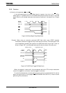
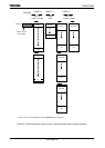
(How to use)
At first, set enable register and using bank-number of each LOCAL register. In that case,
set a combination pin and memory setting to the Ports and Memory controller. After that, if
CPU or LCDC access to logical address of the local area, MMU converts logical address to
physical address according to the bank number, and output it. The physical address is
output to the external address bus pin. By this operation, accessing to external memory
becomes possible. And, if accessed same logical address, physical address is changed by
bank that be set to register in program, and enable accessing that memory of other bank.
Note:
1) When set the bank page, it inhibit to set overlapped area with common area ( because Local area
and common area shows same physical address)
2) In the LOCAL-area, changing Program bank number (LOCALPX, Y or Z) is disabled. Program bank
setting of each local area must change in common area. (But bank setting of data-Read, data-Write
and LCDC-display data can change also in local area.)
3) After data bank number (LOCALRn, LOCALWn or LOCALLn, LOCALEDn, LOCALSn, LOCALODn;
“n” means X, Y or Z) register is set by an instruction, don’t access its memory by next instruction
because of some clocks are needed to be effective MMU setting. In this case, insert dummy
instruction which accesses SFR or another memory between them like following example.
(Example) ld xix, 200000h ;
ldw (localrx), 8001h ; read-data bank number is set
ldw wa, (localrx)
; <---- Inserted Dummy instruction which accesses SFR
ldw wa, (xix) ; instruction which reads bank1 of local-X area.
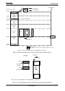
4) When LOCAL-Z area is used, Chip select signal
CSZA should be assigned to P82-pin.
In this case,
CSZA works as chip select signal for not only bank0 to 15 but also COMMON-Z.
But for it, following setting after reset is needed before P82 setting.
ldw (localpz), 8000h ; LOCAL-Z Bank enable for program
ldw (localrz), 8000h ; LOCAL-Z Bank enable for data read
ldw (localwz), 8000h ; LOCAL-Z Bank enable for data write (*1)
ldw (locallz), 8000h ; LOCAL-Z Bank enable for LCD display memory (*2)
ld (p8fc), -----0--B ; Assign P82 to
CSZA
ld (p8fc2), -----1--B ;
(*1) If COMMON-Z area is not used as data write memory, this setting is not needed.
(*2) If COMMON-Z area is not used as LCD display memory, this setting is not needed.