


TMP92CZ26A
92CZ26A-73
If micro DMA requests are set simultaneously for more than one channel, priority is
not based on the interrupt priority level but on the channel number: The lower the
channel number, the higher the priority (Channel 0 thus has the highest priority and
channel 7 the lowest).
Note: Don’t start any micro DMAs by one interrupt. If any micro DMA are set by it, micro DMA that
channel number is biggest (priority is lowest) is not started.(Because interrupt flag is
cleared by micro DMA that priority is highest)
Although the control registers used for setting the transfer source and transfer
destination addresses are 32 bits wide, this type of register can only output 24-bit
addresses. Accordingly, micro DMA can only access 16 Mbytes (The upper 8 bits of a
32-bit address are not valid).
Three micro DMA transfer modes are supported: 1byte transfer, 2byte (One word)
transfers and 4byte transfers. After a transfer in any mode, the transfer source and
transfer destination addresses will either be incremented or decremented, or will
remain unchanged. This simplifies the transfer of data from memory to memory, from
I/O to memory, from memory to I/O, and from I/O to I/O. For details of the various
transfer modes, see section 3.5.2 (4) “Detailed description of the transfer mode
register”.
Since a transfer counter is a 16-bit counter, up to 65536 micro DMA processing
operations can be performed per interrupt source (Provided that the transfer counter
for the source is initially set to 0000H).
Micro DMA processing can be initiated by any one of 48 different interrupts – the 47
interrupts shown in the micro DMA start vectors in
Table 3.5.1 and a micro DMA soft
start.
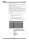
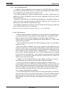
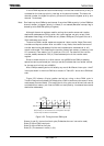
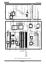
Figure 3.5.2 shows a 2-byte transfer carried out using a micro DMA cycle in
Transfer Destination Address INC Mode (micro DMA transfers are the same in every
mode except Counter Mode). (The conditions for this cycle are as follows: both source
and destination memory are internal-RAM and multipled by 4 numbered source and
destination addresses).
src
1 state
f
SYS
A23 to 0
(1)
dst
(2) (3) (4) (5)
(Note) Actually, src and dst address are not outputted to A23-0 pins
because they are address of internal-RAM.
Figure 3.5.2 Timing for micro DMA cycle
States (1) and (2): Instruction fetch cycle (Prefetches the next instruction code)
State (3): Micro DMA read cycle.
State (4): Micro DMA write cycle.
State (5): (The same as in state (1), (2).)